RF2681 데이터 시트보기 (PDF) - RF Micro Devices
부품명
상세내역
일치하는 목록
RF2681 Datasheet PDF : 8 Pages
| |||
RF2681
Preliminary
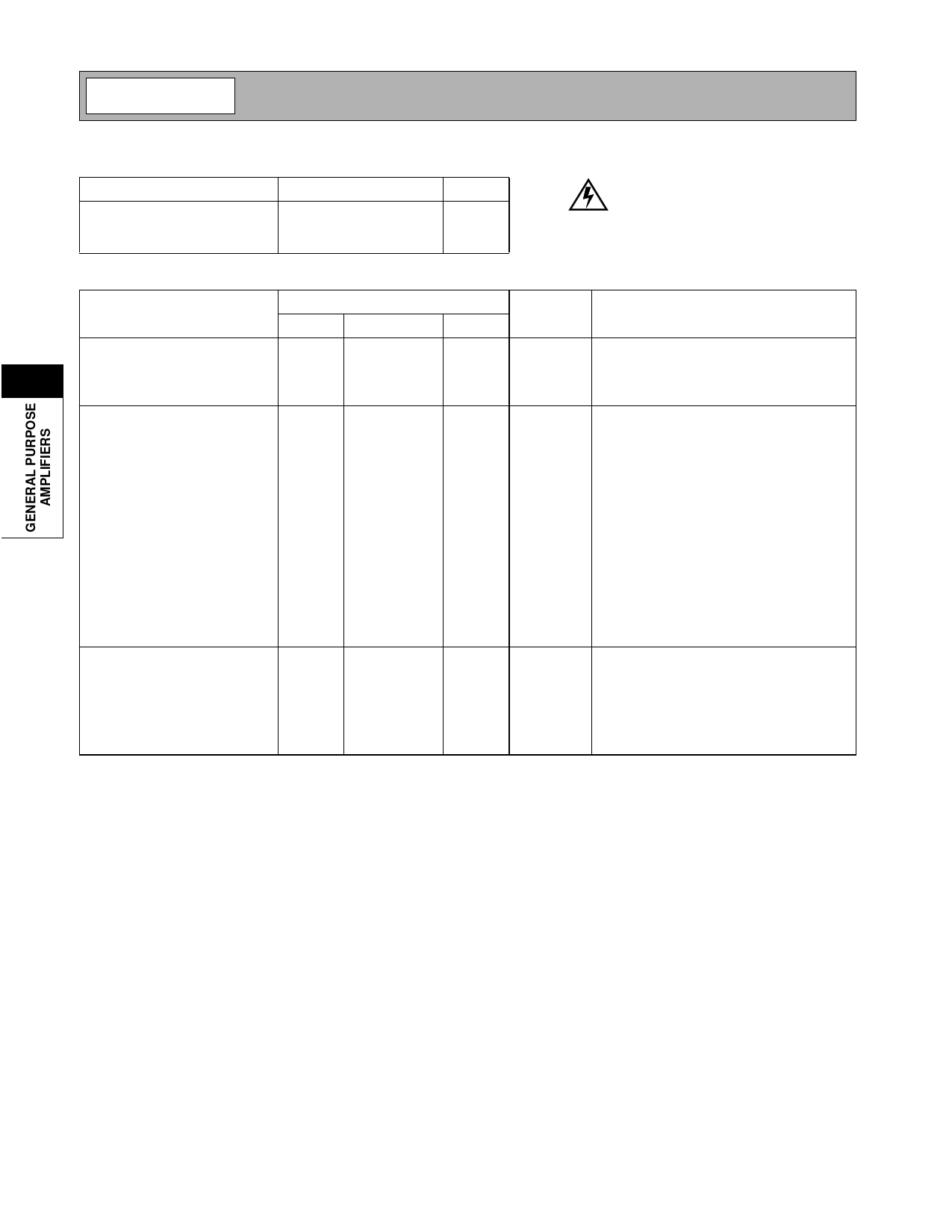
Absolute Maximum Ratings
Parameter
Supply Voltage
Operating Ambient Temperature
Storage Temperature
Rating
-0.5 to +3.6
-40 to +85
-40 to +150
Unit
VDC
°C
°C
Caution! ESD sensitive device.
RF Micro Devices believes the furnished information is correct and accurate
at the time of this printing. However, RF Micro Devices reserves the right to
make changes to its products without notice. RF Micro Devices does not
assume responsibility for the use of the described product(s).
Parameter
Overall
Usable Frequency Range
4
Linear Gain Control Range
Gain Control Slope
W-CDMA
Operating Frequency
Small Signal Gain
Specification
Min.
Typ.
Max.
1800 to 2100
30
40
1920 to 1980
24
26
29
-7
-5
-3
Unit
Condition
MHz
dB
dB/V
MHz
dB
VGC=2.4V (Maximum Gain)
VGC=0V (Minimum Gain)
Output IP3
Noise Figure
Input VSWR
Output VSWR
Maximum Linear Output Power
ACPR1 (5MHz Offset)
+22.0
8
ACPR2 (10MHz Offset)
Power Supply
Supply Voltage
Gain Control Voltage
Supply Current
VGC Current
+24.0
3
1.4:1
1.8:1
9
2.7
0 to 2.4
38
220
1.7
+26.0
2:1
2:1
-48
-62
3.3
dBm
dB
dBm
dBc
dBc
V
V
mA
µA
mA
VGC=2.4V (Maximum Gain)
Small signal
Over entire gain control range
W-CDMA ACPR<-43dBc
Over entire gain control range. PIN such that
POUT=9dBm at maximum gain setting.
W-CDMA reverse link modulation.
Operating range
Useful range
VCC = 2.7 V
VGC=2.4V (Maximum Gain)
VGC = 0.2 V
4-44
Rev A1 010824
Share Link: 