NJM592D8 데이터 시트보기 (PDF) - Japan Radio Corporation
부품명
상세내역
일치하는 목록
NJM592D8 Datasheet PDF : 6 Pages
| |||
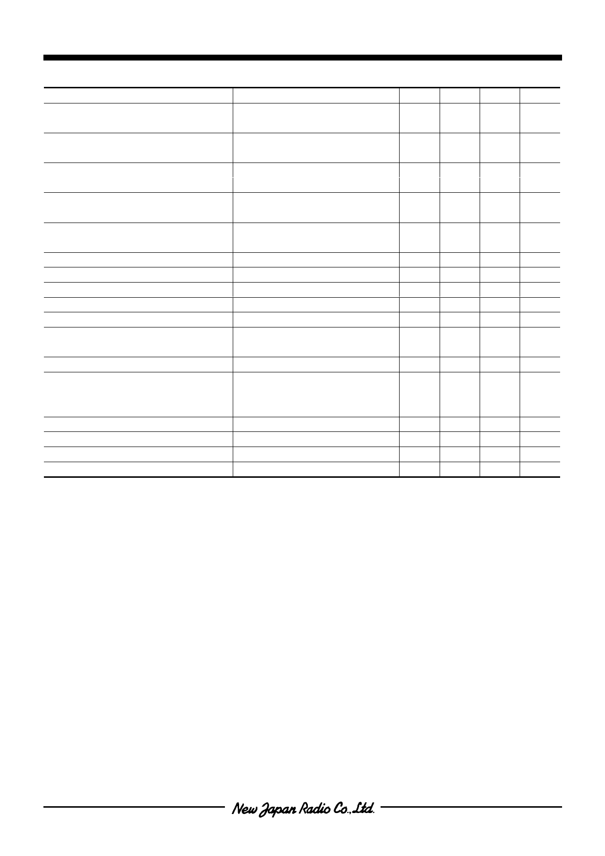
■ ELECTRICAL CHARACTERISTICS
PARAMETER
TEST CONDITION
Differential Voltage Gain 1 (note 1)
R1=2kΩ, VOUT=3VP-P
Differential Voltage Gain 2 (note 2, 4)
Bandwidth (note 1)
Bandwidth 2 Gain 2 (note 2, 4)
Rise Time Gain 1 (note 1)
VOUT =1VP-P
Rise Time Gain 2 (note 2, 4)
Propagation Delay 1 Gain 1 (note 1)
VOUT =1VP-P
Propagation Delay 2 Gain 2 (note 2, 4)
Input Resistance Gain 1 (note1)
Input Resistance Gain 2 (note 2, 4)
Input Capacitance Gain 2 (note2, 4)
Input Offset Current
Input Bias Current
Input Noise Voltage
BW=1kHz to 10MHz
Input Voltage Range
Common Mode Rejection Radio Gain 2 (note 4) VCM=±1V, f<100kHz
Common Mode Rejection Radio Gain 2 (note 4) VCM=±1V, f=5MHz
Supply Voltage Rejection Radio Gain 2 (note ▪) ∆V+/V=±0.5V
Output Offset Voltage Gain 1 (note 1)
RL=∞
Output Offset Voltage Gain 2 (note2, 4)
RL=∞
Output Offset Voltage Gain 3 (note 3)
RL=∞
Output Common Mode Voltage
RL=∞
Output Voltage Swing
RL=2kΩ
Output Resistance
Output Current
RL=∞
(note 1) : Gain select pins G1A and G1B connected together. (Gain 1)
(note 2) : Gain select pins G2A and G2B connected together. (Gain 2)
(note 3) : All gain select pins open.
(note 4) : Apply to only 14 pins package.
NJM592
(Ta=25°C, V+=±6V, VCM=0)
MIN. TYP. MAX. UNIT
250
400
600
V/V
80
100
120
-
40
-
MHz
-
90
-
-
10.5
-
ns
-
4.5
-
7.5
-
ns
-
6.0
-
-
4.0
-
kΩ
-
30
-
-
2.0
-
pF
-
0.4
5.0
µA
-
9.0
30
µA
-
12
-
µVrms
-
-
±1.0
V
60
86
-
dB
-
60
-
50
70
-
dB
-
-
1.5
-
-
1.5
V
-
0.35
0.75
2.4
2.9
3.4
V
3.0
4.0
-
V
-
20
-
Ω
-
18
24
mA
Ver.2004-02-17
-3-
Share Link: 