L4922 데이터 시트보기 (PDF) - STMicroelectronics
부품명
상세내역
일치하는 목록
L4922 Datasheet PDF : 6 Pages
| |||
L4922
ABSOLUTE MAXIMUM RATINGS
Symbol
Vi
Vr
VD
TJ
Top
Tstg
Parameter
DC Input Voltage
DC Reverse Voltage
Positive Load Dump Protection (t = 300ms)
Junction Temperature Range
Operating Temperature Range
Storage Temperature Range
N ote: T he circuit is ESD protected according to MIL-STD -883C
THERMAL DATA
Symbol
Parameter
Rth j-case Thermal Resistance Junction-case
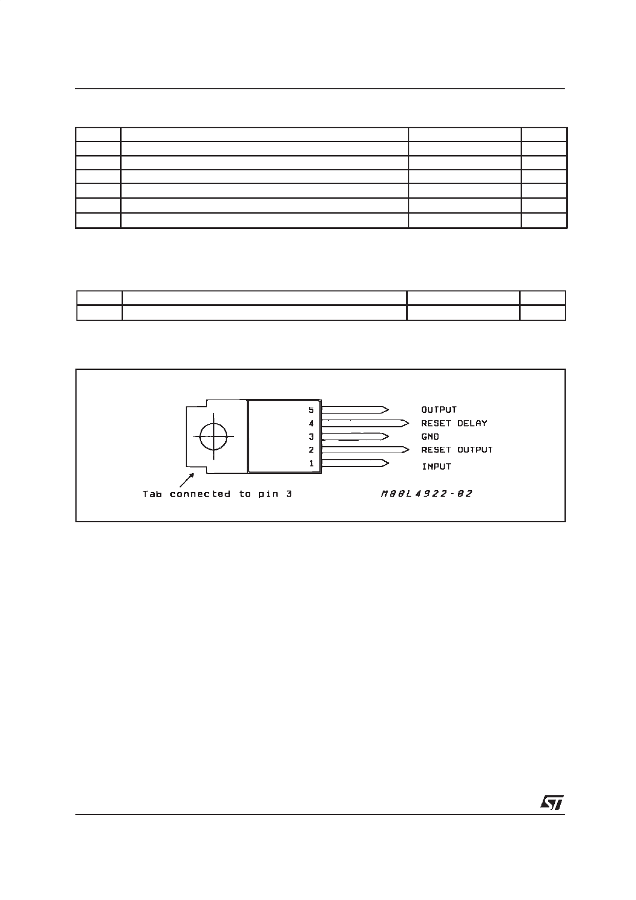
PIN CONNECTION (Top view)
Value
Unit
35
V
–18
V
60
V
–40 to 150
°C
–40 to 125
°C
–55 to 150
°C
Max.
Value
3.5
Unit
°C/W
FUNCTIONAL DESCRIPTION
The operating principle of the voltage regulator is
basedon thereference,the error amplifier,the driver
and the power PNP. This stage uses an Isolated
CollectorVertical PNP transistor which allowsto ob-
tain very low dropout voltage (typ. 450mV) and low
quiescent current (IQ = 20mA typically at Io = 1A).
Thanks to these features the device is particularly
suited when the power dissipation must be limited
as, for example, in automotive or industrial applica-
tions supplied by battery.
The three gain stages (operational amplifier,
driver and power PNP) require the external capaci-
tor (Comin = 22µF) to guarantee the global stability
of the system.
The antisaturationcircuit allowsto reduce drastically
the current peak which takes place during the start
up.
The reset function is LOW active when the output
voltage level is lower than the reset threshold volt-
age VRthOFF (typ.value : Vo – 150mV).When the out-
put voltage is higher thanVRthON the reset becomes
HIGH aftera delaytime settablewith the externalca-
pacitorCd. Typicallytd =20ms, Cd = 0.1µF. The reset
and delay threshold hysteresis improve the noise
immunity allowing to avoid false switchings. The
typical reset output waveform is shown in fig. 1.
2/6
Share Link: 