MC74AC190N 데이터 시트보기 (PDF) - Motorola => Freescale
부품명
상세내역
일치하는 목록
MC74AC190N Datasheet PDF : 8 Pages
| |||
CP U/D
P0
CE
MC74AC190
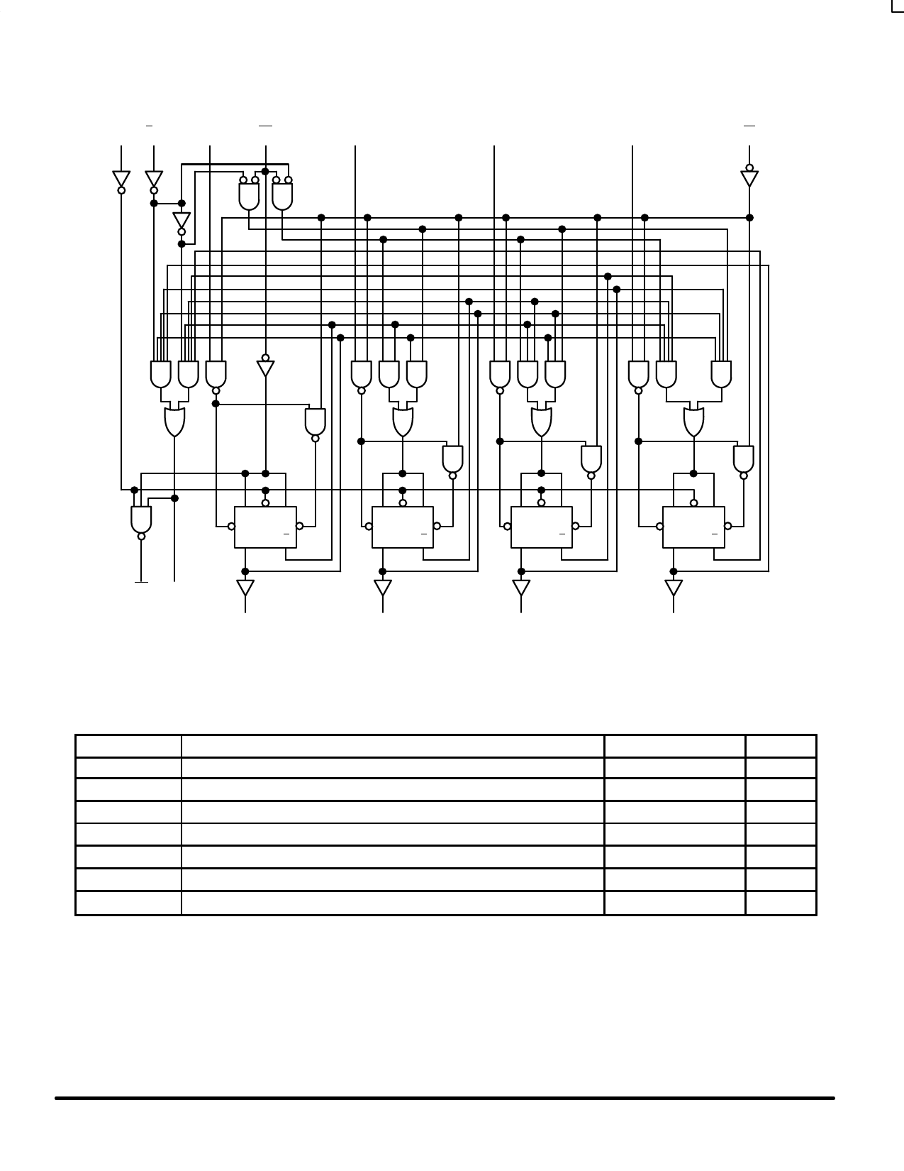
LOGIC DIAGRAM
P1
P2
P3
PL
RC TC
J CLOCK K
PRESET
CLEAR
Q
Q
J CLOCK K
PRESET
CLEAR
Q
Q
J CLOCK K
PRESET
CLEAR
Q
Q
J CLOCK K
PRESET
CLEAR
Q
Q
Q0
Q1
Q2
Q3
Please note that this diagram is provided only for the understanding of logic
operations and should not be used to estimate propagation delays.
MAXIMUM RATINGS*
Symbol
Parameter
Value
Unit
VCC
Vin
Vout
Iin
Iout
ICC
Tstg
DC Supply Voltage (Referenced to GND)
DC Input Voltage (Referenced to GND)
DC Output Voltage (Referenced to GND)
DC Input Current, per Pin
DC Output Sink/Source Current, per Pin
DC VCC or GND Current per Output Pin
Storage Temperature
–0.5 to +7.0
V
–0.5 to VCC +0.5
V
–0.5 to VCC +0.5
V
±20
mA
±50
mA
±50
mA
–65 to +150
°C
* Maximum Ratings are those values beyond which damage to the device may occur. Functional operation should be restricted to the Recommended
Operating Conditions.
FACT DATA
5-4
Share Link: 