HEF4053BPB 데이터 시트보기 (PDF) - NXP Semiconductors.
부품명
상세내역
일치하는 목록
HEF4053BPB Datasheet PDF : 20 Pages
| |||
NXP Semiconductors
HEF4053B
Triple single-pole double-throw analog switch
Table 7. ON resistance …continued
Tamb = 25 C; ISW = 200 A; VSS = VEE = 0 V.
Symbol Parameter
Conditions
VDD VEE Typ
RON(rail) ON resistance (rail)
VI = 0 V; see Figure 10 and Figure 11 5 V
115
10 V
50
15 V
40
VI = VDD VEE;
see Figure 10 and Figure 11
5V
120
10 V
65
15 V
50
RON
ON resistance mismatch VI = 0 V to VDD VEE; see Figure 10 5 V
25
between channels
10 V
10
15 V
5
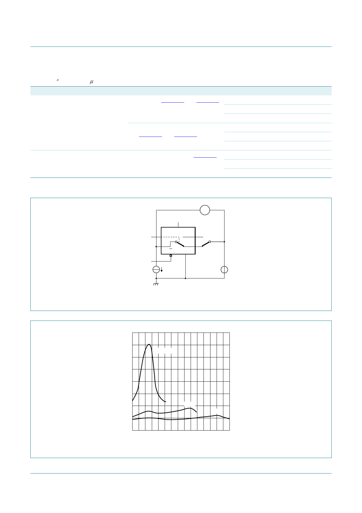
10.2.1 ON resistance waveform and test circuit
Max
Unit
340
160
115
365
200
155
-
-
-
VDD or VSS
VSS
RON = VSW / ISW.
Fig 10. Test circuit for measuring RON
VDD
V
VSW
S1 to S3
nZ
E
nY0 1
nY1 2
switch
VSS = VEE
ISW
VI
001aaj902
400
RON
(Ω)
300
VDD = 5 V
001aae648
200
100
10 V
15 V
0
0
5
Fig 11. Typical RON as a function of input voltage
10
15
VI (V)
HEF4053B
Product data sheet
All information provided in this document is subject to legal disclaimers.
Rev. 10 — 17 November 2011
© NXP B.V. 2011. All rights reserved.
7 of 20
Share Link: 