NJU6624C 데이터 시트보기 (PDF) - Japan Radio Corporation
부품명
상세내역
일치하는 목록
NJU6624C
Japan Radio Corporation

NJU6624C Datasheet PDF : 27 Pages
| |||
NJU6624C
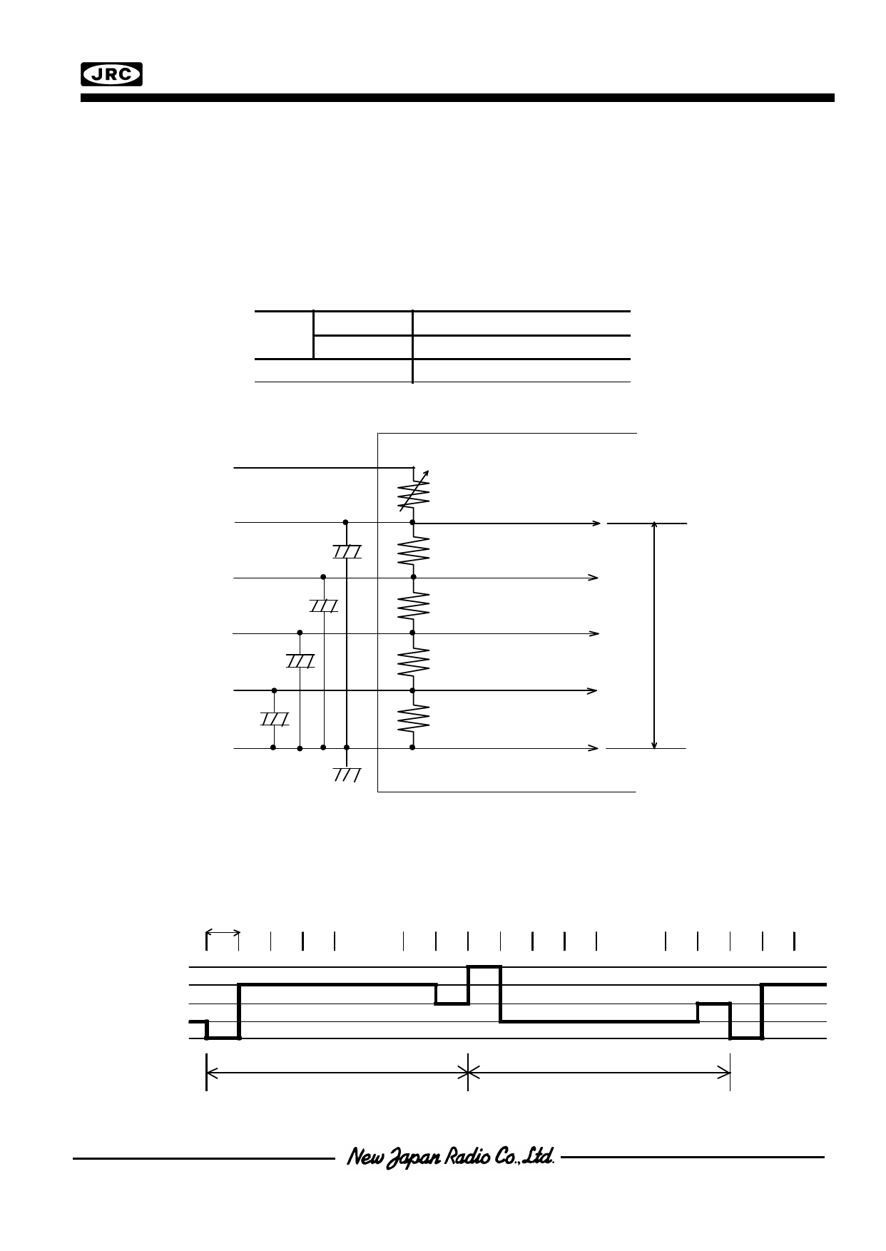
(5)LCD display
(5-1)Bleeder Resistance
Each LCD driving voltage ( V1, V2, V3, V4 ) is LCD driving high voltage input to the VLCD1 terminal, generated by
the E.V.R. and high impedance bleeder resistance.
The bleeder resistance is set 1/4 bias suitable for 1/8 duty ratio.
The capacitor connected between VLCD2 and VSS is needed for stabilizing VLCD. The determination of the each
capacitance requires to operate with the LCD panel actually.
LCD Driving Voltage vs Duty Ratio
Power Duty Ratio
1/8
supply
Bias
1/4
V LCD
VLCD2- VSS
VLCD is the maximum amplitude for LCD driving voltage.
VLCD1
VLCD2
V1
V2
V4
VSS
+
+
+
+
Internal NJU6624
E.V.R.(16Step)
5K
VLCD
4K
V1
4K
V2 (V3)
4K
V4
4K
VSS
VLCD
(5-2)Relation between oscillation frequency and LCD frame frequency
As the NJU6624C incorporate oscillation capacitor and resistor for CR oscillation, 145kHz oscillation is available
without any external components.
The LCD frame frequency example mentioned below is based on 145kHz oscillation.(1clock =6.90us)
224clocks
Icon 1
2
3
.............. 7 K e y Icon 1
2
3
.............. 7 K e y Icon 1 2
VLCD
V1
COM1 V2
V4
VSS
1 frame
1 frame
1 frame = 6.90(us) x 224 x 8 = 12.36(ms)
Frame frequency = 1 / 12.36(ms) = 79.50(Hz)
Key scan time = 220.70(uS)
Share Link: