M66305AFP 데이터 시트보기 (PDF) - MITSUBISHI ELECTRIC
부품명
상세내역
일치하는 목록
M66305AFP Datasheet PDF : 10 Pages
| |||
MITSUBISHI 〈DIGITAL ASSP〉
M66305AP/AFP
TOGGLE LINE BUFFER
FUNCTION
When the status of input clock enable (ICE) is “L”, input data
(SIDATA) is taken in (written) synchronously with input clock
(SICLK) rise edge. When output clock enable (OCE) is “L”,
output data (SODATA) is output (read) synchronously with
output clock (SOCLK) fall edge. The double buffer system
makes independent read and write operation possible.
When one-line write and one-line read are completed, toggle
signal (T) is required to be changed to “L”, With input of toggle
signal, the line buffer memory which has completed write op-
eration is switched to read mode, and the line buffer which
has completed output is switched to write mode, enabling
next write and read operations.
To rewrite data during write operation, use write counter re-
set input (CNTRST1). To repeat output during output opera-
tion, use read counter reset (CNTRST2).
These operations are possible only when the status of chip
select (CS) is “L”.
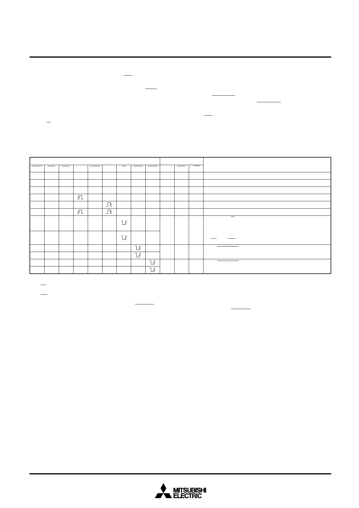
FUNCTION TABLE
Input
Output
RES CS ICE SIC OCE SOC T CR1 CR2 SOD INT BF
Remarks
L X X X X X X X X L H H Initialization
H H X X X X X X X Q0 Q0 Q0 No internal change, no output change
H L H X H X H H H Q0 Q0 Q0 No internal change, no output change
HL L
H X H H H Q0 Q0 *1 With rise of SICLK, data is written on line buffer memory.
H L HX L
H H H *2 *3 Q0 With fall of SOCLK, data is output.
HL L
L
H H H *2 *3 *1 Write and read
HL L LXL
H L HXX L
HH
With rise of T:
1) Line buffer memory in read mode is switched to write
*4 H H
mode and the other in write mode is switched to read
HH
mode.
2) BF and INT are canceled.
HL L LXXH
HLHXXXH
H
H
*5
*5
H
With CNTRST1 input, internal write counter is reset,
enabling rewriting.
HL XX L LHH
HL XXHXHH
*6
H
*6
With CNTRST2 input, internal read counter is reset,
enabling retrial of output.
Q0 : No change
x : “H” or “L”
*1 : BF changes from “H” to “L” with rise of SICLK for write of 5120th bit.
*2 : With fall of SOCLK, data written before toggle signal input is output in order.
*3 : INT changes from “H” to “L” when the status of SOCLK rises after output of final bit of written before toggle signal inputs.
*4 : Outputs the first bit of written data (D0).
*5 : Output operation can be performed irrespective of CNTRST1.
*6 : SODATA changes to the first bit of written data (D0). Write operation can be performed irrespective of CNTRST2.
2
Share Link: 