PI74SSTV16857A 데이터 시트보기 (PDF) - Pericom Semiconductor
부품명
상세내역
일치하는 목록
PI74SSTV16857A Datasheet PDF : 6 Pages
| |||
PI74SSTV16857
14-Bit Registered Buffer 1122334455667788990011223344556677889900112233445566778899001122112233445566778899001122334455667788990011223344556677889900112211223344556677889900112233445566778899001122334455667788990011221122334455667788990011223344556677889900112233445566778899001122112233445566778899001122
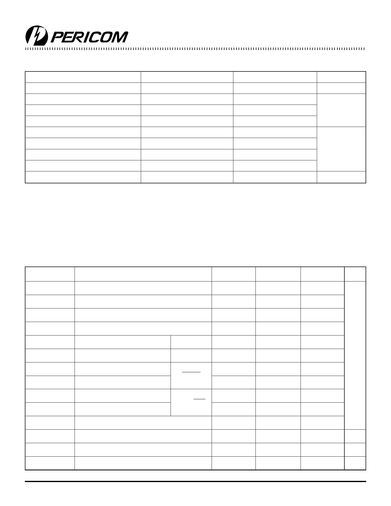
Maximum Ratings
(Above which the useful life may be impaired. For user guidelines, not tested.)
Item
Storage temperature
Supply voltage
Input voltage(1)
Output voltage(1,2)
Input clamp current
Output clamp current
Continuous output current
VDD, VDDQ or GND current/pin
Package Thermal Impedance(3)
Symbol/Conditions
Tstg
VDD or VDDQ
VI
VO
IIK, VI<0
IOK, VO<0
IO, VO = 0 to VDDQ
IDD, IDDQ or IGND
θJA
Ratings
65 to 150
0.5 to 3.6
0.5 to VDD +0.5
0.5 to VDDQ +0.5
50
±50
±50
±100
70
Units
°C
V
mA
°C/W
Note:
Stresses greater than those listed under MAXIMUM RATINGS may cause permanent damage to the device. This is a stress rating only
and functional operation of the device at these or any other conditions above those indicated in the operational sections of this
specification is not implied. Exposure to absolute maximum rating conditions for extended periods may affect reliability.
Notes:
1. The input and output negative voltage ratings may be excluded if the input and output clamp ratings are observed.
2. This current will flow only when the output is in the high state level VO > VDDQ.
3. The package thermal impedance is calculated in accordance with JESD 51.
Recommended Operating Conditions
Parameters
Description
Min.
Nom.
Max.
Units
VDD
VDDQ
VREF
VTT
VIH
VIL
VIH
VIL
VIN
VID
VIX
IOH
IOL
TA
Supply Voltage
I/O Supply Voltage
Reference Voltage VREF = 0.5X VDDQ
Termination Voltage
DC Input High Voltage
Data Inputs
DC Input Low Voltage
Input High Voltage
Input Low Voltage
RESET
Input Voltage Level
Input Differential Voltage
CLK,CLK
Cross Point Voltage of Differential Clock Pair
High-Level Output Current
Low-Level Output Current
Operating Free-Air Temperature
2.3
2.3
1.15
VREF 0.04
VREF +0.15
0.3
1.7
0.3
0.3
0.36
(VDDQ/2) 0.2
20
20
0
2.5
2.5
1.25
VREF
2.7
2.7
1.35
VREF +0.04
VDDQ +0.3
VREF 0.15
V
VDDQ +0.3
0.8
VDDQ +0.6
(VDDQ/2) +0.2
mA
70
ºC
PS8460C 06/04/01
2
Share Link: 