NJG1520PE1-L1 데이터 시트보기 (PDF) - Japan Radio Corporation
부품명
상세내역
일치하는 목록
NJG1520PE1-L1 Datasheet PDF : 17 Pages
| |||
NJG1520PE1
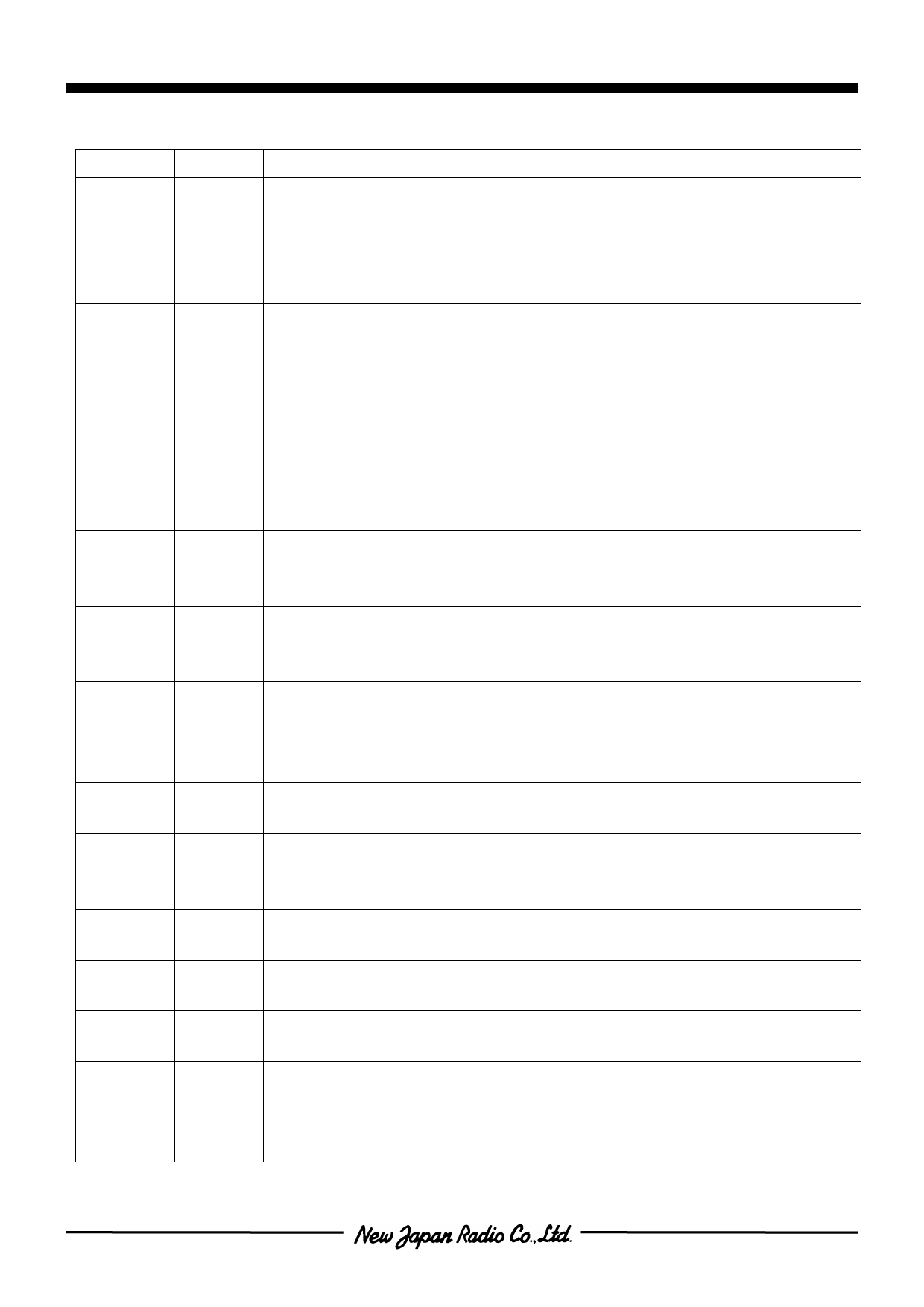
nTERMINAL INFORMATION
PIN No.
1
2
3
5
6
10
12
14
16
17
19
21
23
4, 7, 8, 9,
11, 13, 15,
18, 20, 22,
24
SYMBOL
VSS
CTL3
CTL2
CTL1
VDD
TER1
RX
ANT1
ANT2
TER2
TX
EXT1
EXT2
GND
DESCRIPTION
Negative voltage supply terminal. Please supply negative voltage of -3.5~-2.0V
on transmitting state. On receiving state, this terminal is internally disconnected,
so the voltage of this terminal(negative, short, or open) does not affect to
receiving signal quality. The bypass capacitor should be connected between this
terminal and GND for excellent RF performance.
High-impedance C-MOS input terminal. This terminal is set to High-Level
(+2V~VDD) or Low-Level (+0.6V~0V). If the voltage level of this terminal is
unstable, please connect a resistor (100KΩ) with GND terminal or VDD terminal.
High-impedance C-MOS input terminal. This terminal is set to High-Level
(+2V~VDD) or Low-Level (+0.6V~0V). If the voltage level of this terminal is
unstable, please connect a resistor (100KΩ) with GND terminal or VDD terminal.
High-impedance C-MOS input terminal. This terminal is set to High-Level
(+2V~VDD) or Low-Level (+0.6V~0V). If the voltage level of this terminal is
unstable, please connect a resistor (100KΩ) with GND terminal or VDD terminal.
Positive voltage supply terminal. The positive voltage (+2.7~+5.0V) have to be
supplied. Please connect a bypass capacitor with GND terminal for excellent RF
performance.
ANT2 termination port. Please connect this port and GND by appropriate
capacitor (5pF) to suppress the interference of ANT2 port signal to ANT1 port.
The capacitor works as DC voltage (VDD) blocking.
RF receiving port. An external capacitor (56pF~100pF) is required to block DC
voltage (VDD) .
RF transmitting/receiving port. An external capacitor (56pF~100pF) is required to
block DC voltage (VDD) .
RF receiving port. An external capacitor (56pF~100pF) is required to block DC
voltage (VDD).
ANT2 termination port. Please connect this port and GND by appropriate
capacitor (10pF) to suppress the interference of ANT1 port signal to ANT2 port.
The capacitor works as DC voltage (VDD) blocking.
RF transmitting port. An external capacitor of 56pF~100pF is required to block
DC voltage (VDD).
RF transmitting/receiving port. An external capacitor of 56pF~100pF is required
to block DC voltage (VDD).
RF receiving port. An external capacitor of 56pF~100pF is required to block DC
voltage (VDD).
Ground terminal. Please connect this terminal with ground plane as close as
possible for excellent RF performance.
-7-
Share Link: 