LT1306 데이터 시트보기 (PDF) - Linear Technology
부품명
상세내역
일치하는 목록
LT1306 Datasheet PDF : 16 Pages
| |||

LT1306
APPLICATIONS INFORMATION
Since a boost converter produces high output current
ripple, one also needs to consider the maximum ripple
current rating of the output capacitor. Capacitor reliability
will be affected if the ripple current exceeds the maximum
allowable ratings. This maximum rating is usually
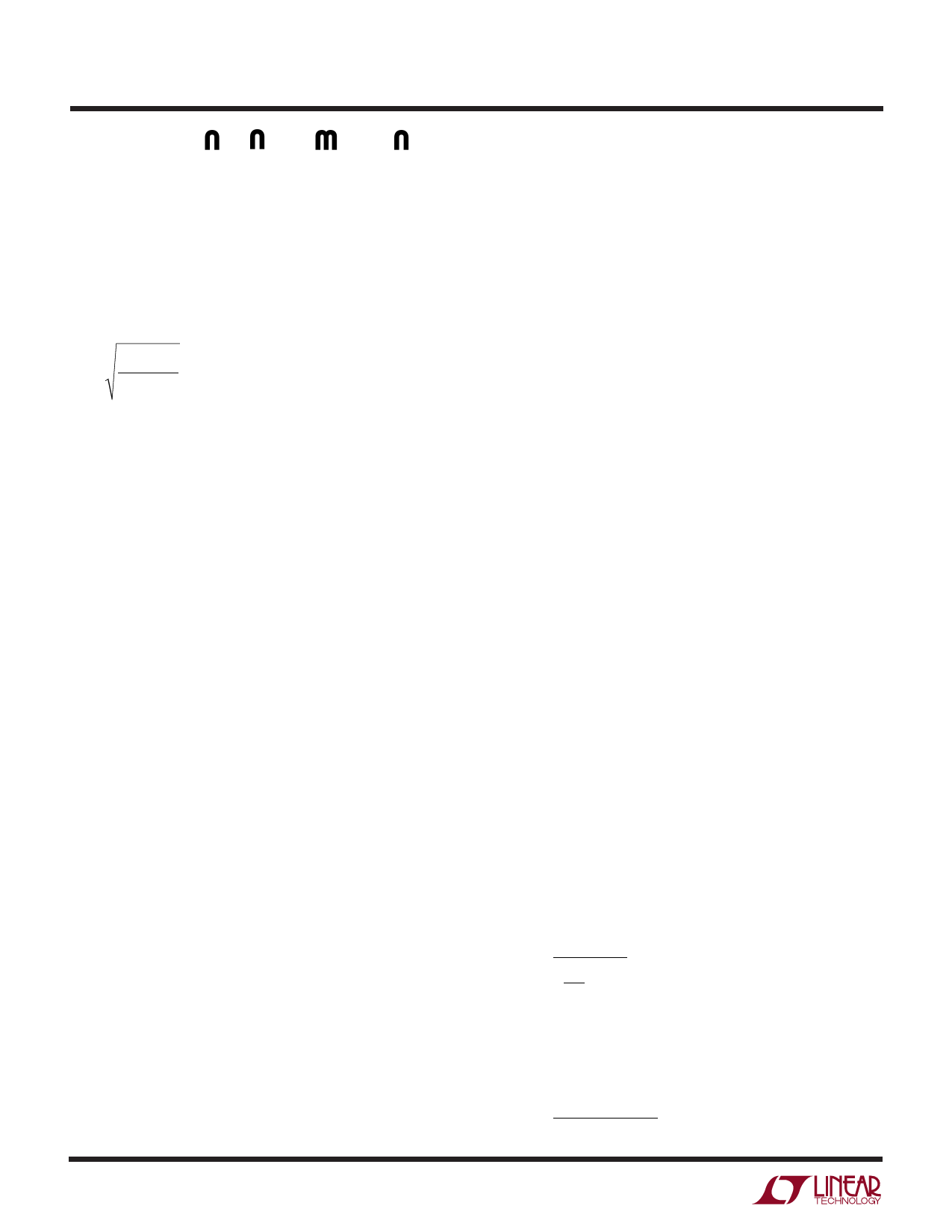
specified as the RMS ripple current. In the LT1306 the
RMS output capacitor ripple current is:
IO
VO – VIN
VIN
For 2-cell to 5V applications, 220µF low ESR solid tanta-
lum capacitors (AVX TPS series or Sprague 593D series)
work well. To reduce output voltage ripple due to heavy
load transients or Burst Mode operation, higher capaci-
tance may be used. For through-hole applications, Sanyo
OS-CON capacitors are also good choices.
In a boost regulator, the input capacitor ripple current is
much lower. Maximum ripple current rating and input
voltage ripples are not usually of concern. A 22µF tantalum
capacitor soldered near the input pin is generally an
adequate bypass.
Bootstrap Supply
Diode D1 and capacitor C1 generate a pulsating supply
voltage, VCAP, which is higher than the output. The rectifier
drive circuit runs off this supply. During rectifier on-time,
the rectifier base current drains C1. Q2 base current and
the maximum allowable VCAP ripple voltage determine the
size of C1. A 1µF capacitor is sufficient to keep VCAP ripple
below 0.3V. For a 2-cell input (VIN > 1.8V) over an extended
temperature range, a BAT54 Schottky diode may be used
for D1. The use of a Schottky diode increases the bootstrap
voltage and the operating headroom for the rectifier driver,
X5. Diodes like a 1N4148 or 1N914 work well for 2-cell
inputs over the 0°C to 70°C commercial temperature
range.
The charge drawn from C1 during the rectifier on-time has
to be replenished during the switch on-interval. As duty
cycle decreases, the amplitude of the C1 charging current
can increase dramatically especially when delivering high
power to the load. This charging current flows through the
switch and can cause the current limit comparator to trip
erratically. For boost applications where VIN is a few tenths
of a volt below VO, a 1µF or 2.2µF tantalum capacitor (such
as AVX TAJ series) can be used for C1. The ESR of the
tantalum capacitor limits the charging current. A low value
resistor (2Ω to 5Ω) can also be added in series with C1 for
further limiting the charging current although this tends to
lower the converter efficiency slightly.
Frequency Compensation
Current mode switching regulators have two feedback
loops. The inner current feedback loop controls the
inductor current in response to the outer loop. The outer
or overall feedback loop tightly regulates the output
voltage. The high frequency gain asymptote of the inner
current loop rolls off at – 20dB/decade and crosses the
unity gain axis at a frequency ωc between 1/6 to 2/3 of the
switching frequency. The current loop is stable and is
wideband compared to the overall voltage feedback loop.
The low frequency current loop gain is not high (usually
between unity and 10) but it increases the low frequency
impedance of the inductor as seen by the output filter
capacitor. (In a boost regulator, the inductor is con-
nected to the output during the switch off-time.) Current
mode control introduces an effective series resistance
(>> DCR) to the inductor that damps the LC tank re-
sponse. The complex high-Q poles of the LC filter are now
separated, resulting in a dominant pole determined by
the filter capacitance and the load resistance and a
second high frequency pole.
For a boost regulator the control to output transfer func-
tion can be shown to have a dominant pole at the load
corner frequency
ωP
=
RL
2
1
(CO )
and a moving right-half plane (RHP) zero with a minimum
value of
ωZ
=
RL(1– DMAX )2
L
10