SL4502B 데이터 시트보기 (PDF) - System Logic Semiconductor
부품명
상세내역
일치하는 목록
SL4502B Datasheet PDF : 5 Pages
| |||
SL4502B
Strobed Hex Inverter/Buffer
High-Voltage Silicon-Gate CMOS
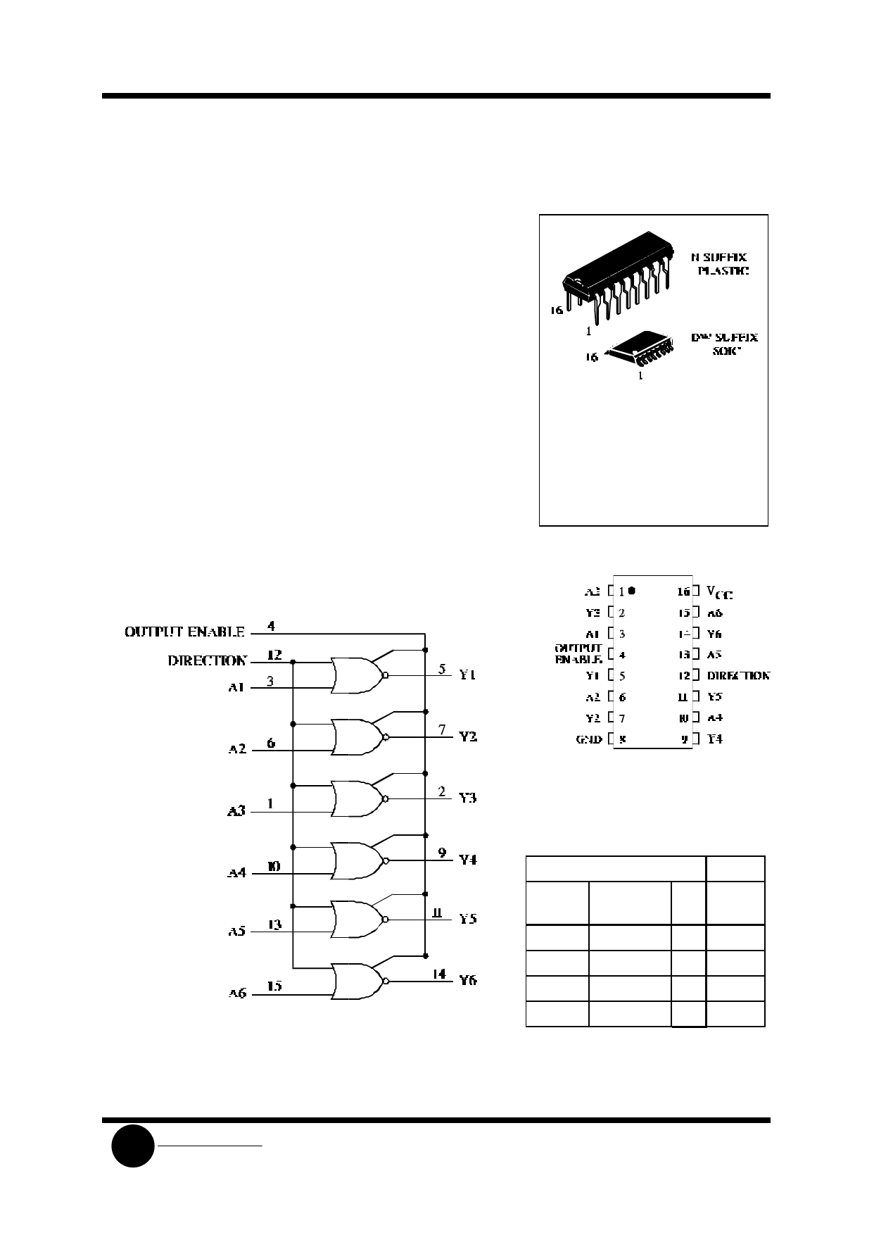
The SL4502B consists of six inverter/buffers with 3-state outputs. A
logic “1” on the OUTPUT ENABLE input produces a high impedance
state in all six outputs. This feature permits common busing of the
outputs, thus simplifying system design. A logic “1” on the
DIRECTION input switches all six outputs to logic “0” if the OUTPUT
ENABLE input is a logic “0”.
• Operating Voltage Range: 3.0 to 18 V
• Maximum input current of 1 µA at 18 V over full package-
temperature range; 100 nA at 18 V and 25°C
• Noise margin (over full package temperature range):
1.0 V min @ 5.0 V supply
2.0 V min @ 10.0 V supply
2.5 V min @ 15.0 V supply
ORDERING INFORMATION
SL4502BN Plastic
SL4502BD SOIC
TA = -55° to 125° C for all packages
LOGIC DIAGRAM
PIN ASSIGNMENT
PIN 16=VCC
PIN 8= GND
SLS
System Logic
Semiconductor
FUNCTION TABLE
Inputs
Output Direction
Enable
L
L
L
L
L
H
H
X
Z = high impedance
X = don’t care
Output
A
Y
L
H
H
L
X
L
X
Z
Share Link: 