NJG1505R-C1 데이터 시트보기 (PDF) - Japan Radio Corporation
부품명
상세내역
일치하는 목록
NJG1505R-C1 Datasheet PDF : 9 Pages
| |||
NJG1505R
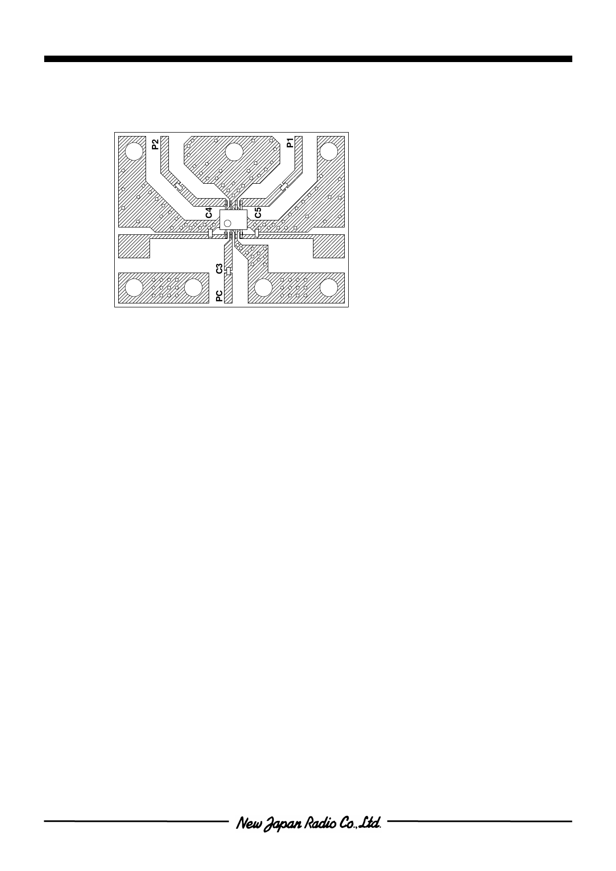
nRECOMMENDED PCB DESIGN
(TOP VIEW)
C1
C2
PCB SIZE=30.0x22.5mm
VCTL2
VCTL1
PCB: FR-4, t=0.5mm
STRIPLINE WIDTH=1mm
CAPACITORS: size 1005
Precautions
[1]
[2]
[3]
[4]
External capacitors should be connected to the input and output RF terminals (P1,
P2, PC) to block the DC current. The values of these capacitors depend on RF
frequency range. Please use a 0.01uF capacitor at 50 to 100MHz, a 0.1uF
capacitor at 100 to 500MHz, and a 56pF capacitor at 500MHz to 2GHz.
Decoupling capacitors should be connected to the control terminals (VCTR1, VCTR2)
as close as possible. The values of these capacitors should be selected to 0.01uF
at 50 to 100MHz, 0.1uF at 100 to 500MHz, and 10pF at 500MHz to 2GHz. Please
take care to select these values because the capacitors make switching time
long.
In order to keep good isolation characteristics, the ground terminals (3, 6, 7 pin)
should be connected to ground pattern with wider width as close as possible, and
through-hole in the ground plane should also be placed as close as possible.
The isolation of PC port to P1 port is greater than the isolation of PC port to P2
port. Please consider this information to create better isolation design.
-8-
Share Link: 