AS1700-PWR 데이터 시트보기 (PDF) - Astec Semiconductor => Silicon Link
부품명
상세내역
일치하는 목록
AS1700-PWR Datasheet PDF : 20 Pages
| |||
AS17xx
Semicustom Bipolar Array
so that they may also be used to create a device
with an integral emitter area ratio with respect to
a standard small NPN.
The AS17xx bipolar array can be packaged in
industry standard DIP or surface mount pack-
ages with 8 to 40 leads. The number of pads
available on the AS17xx varies with the number
of tiles used as follows: single tile per die = 18
pads, two tiles per die = 30 pads, and four tiles
per die = 40 pads. The extra pads not used for
bonding to leads can be used for wafer level
testing, trimming, and debugging.
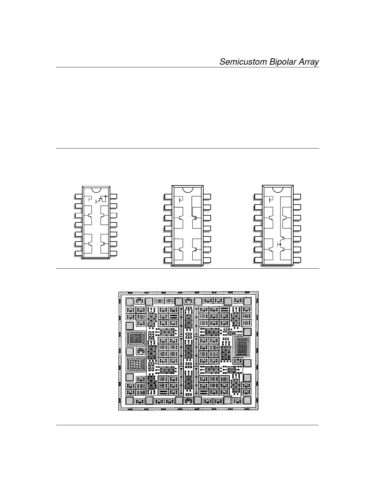
Pin Configuration — Top view
PDIP (N)
AS1700-NPN Kit Part
PDIP (N)
AS1700-PNP Kit Part
SUB 1
C2
B3
E4
C5
B6
E7
14 Vbe
13 C
12 B
11 E
10 C
9B
8E
SUB 1
C2
B3
E4
C5
B6
E7
14 C
13 C
12 B
11 E
10 C
9B
8E
Die Configuration — Top view
PDIP (N)
AS1700-PWR Kit Part
SUB 1
C2
B3
E4
C5
B6
E7
14 E
13 C
12 B
11 E
10 B
9B
8E
ASTEC Semiconductor
Figure 1. Single Tile Bipolar Array
120
Share Link: 