MC-4R128FKE8D-745 데이터 시트보기 (PDF) - Elpida Memory, Inc
부품명
상세내역
일치하는 목록
MC-4R128FKE8D-745 Datasheet PDF : 14 Pages
| |||
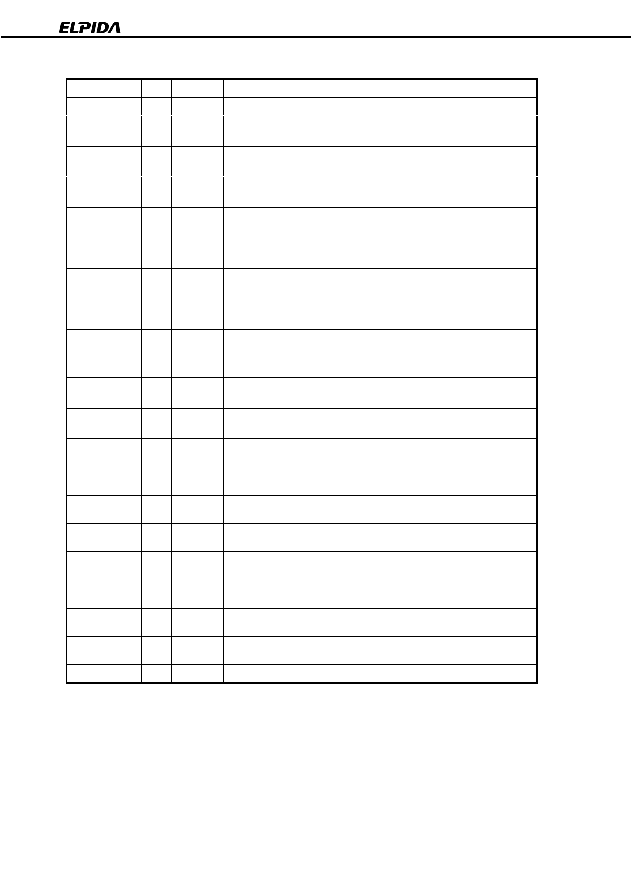
MC-4R128FKE8D
Module Connector Pad Description
(1/2)
Signal
I/O
GND
–
LCFM
I
LCFMN
I
LCMD
I
LCOL4..LCOL0
I
LCTM
I
LCTMN
I
LDQA8..LDQA0 I/O
LDQB8..LDQB0 I/O
LROW2..LROW0 I
LSCK
I
NC
–
RCFM
I
RCFMN
I
RCMD
I
RCOL4..RCOL0
I
RCTM
I
RCTMN
I
RDQA8..RDQA0 I/O
RDQB8..RDQB0 I/O
RROW2..RROW0 I
Type
–
RSL
RSL
VCMOS
RSL
RSL
RSL
RSL
RSL
RSL
VCMOS
–
RSL
RSL
VCMOS
RSL
RSL
RSL
RSL
RSL
RSL
Description
Ground reference for RDRAM core and interface. 72 PCB connector pads.
Clock from master. Interface clock used for receiving RSL signals from the
Channel. Positive polarity.
Clock from master. Interface clock used for receiving RSL signals from the
Channel. Negative polarity.
Serial Command used to read from and write to the control registers. Also used
for power management.
Column bus. 5-bit bus containing control and address information for column
accesses.
Clock to master. Interface clock used for transmitting RSL signals to the
Channel. Positive polarity.
Clock to master. Interface clock used for transmitting RSL signals to the
Channel. Negative polarity.
Data bus A. A 9-bit bus carrying a byte of read or write data between the Channel
and the RDRAM. LDQA8 is non-functional on modules with x16 RDRAM devices.
Data bus B. A 9-bit bus carrying a byte of read or write data between the Channel
and the RDRAM. LDQB8 is non-functional on modules with x16 RDRAM devices.
Row bus. 3-bit bus containing control and address information for row accesses.
Serial clock input. Clock source used to read from and write to the RDRAM
control registers.
These pads are not connected. These 24 connector pads are reserved for future
use.
Clock from master. Interface clock used for receiving RSL signals from the
Channel. Positive polarity.
Clock from master. Interface clock used for receiving RSL signals from the
Channel. Negative polarity.
Serial Command Input used to read from and write to the control registers. Also
used for power management.
Column bus. 5-bit bus containing control and address information for column
accesses.
Clock to master. Interface clock used for transmitting RSL signals to the
Channel. Positive polarity.
Clock to master. Interface clock used for transmitting RSL signals to the
Channel. Negative polarity.
Data bus A. A 9-bit bus carrying a byte of read or write data between the Channel
and the RDRAM. RDQA8 is non-functional on modules with x16 RDRAM devices.
Data bus B. A 9-bit bus carrying a byte of read or write data between the Channel
and the RDRAM. RDQB8 is non-functional on modules with x16 RDRAM devices.
Row bus. 3-bit bus containing control and address information for row accesses.
Data Sheet E0078N20 (Ver 2.0)
5
Share Link: 