CD4034BMS 데이터 시트보기 (PDF) - Intersil
부품명
상세내역
일치하는 목록
CD4034BMS Datasheet PDF : 14 Pages
| |||
CD4034BMS
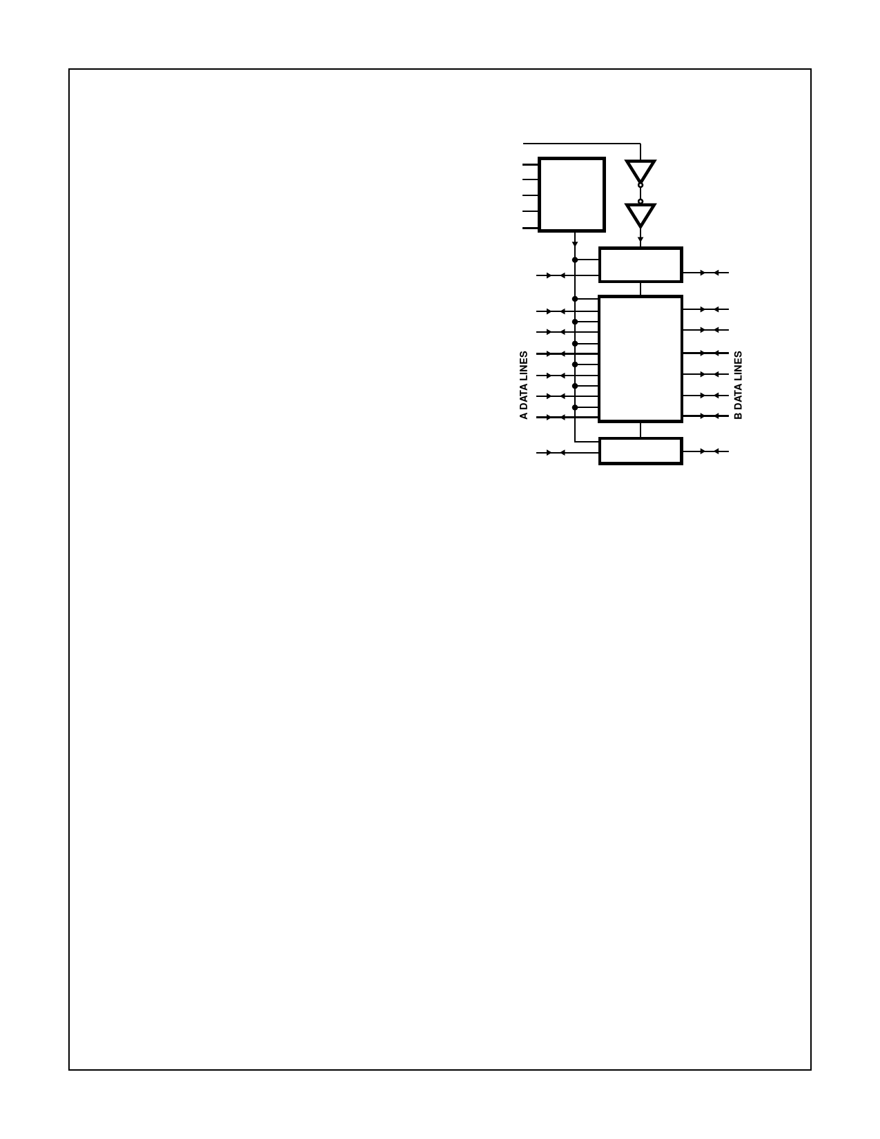
Parallel Operation
Functional Diagram
A high P/S input signal allows data transfer into the register
via the parallel data lines synchronously with the positive
transition of the clock provided the A/S input is low. If the A/S
input is high the transfer is independent of the clock. The
direction of data flow is controlled by the A/B input. When
this signal is high the A data lines are inputs (and B data
lines are outputs); a low A/B signal reverses the direction of
data flow.
SI
AE
A/B
STEERING
LOGIC
A/S
P/S
CL
The AE input is an additional feature which allows many reg-
isters to feed data to a common bus. The A DATA lines are
enabled only when this signal is high.
Data storage through recirculation of data in each register
stage is accomplished by making the A/B signal high and the
AE signal low.
Serial Operation
SI
A1 Q B1
SI
6
STAGES
A low P/S signal allows serial data to transfer into the regis-
ter synchronously with the positive transition of the clock.
The A/S input is internally disabled when the register is in
the serial mode (asynchronous serial operation is not
allowed).
Q
SI
A8
B8
The serial data appears as output data on either the B lines
(when A/B is high) or the A lines (when A/B is low and the
AE signal is high).
Register expansion can be accomplished by simply cascad-
ing CD4034BMS packages.
The CD4034BMS is supplied in these 24 lead outline pack-
ages:
Braze Seal DIP H4V
Ceramic Flatpack H4P
7-838
Share Link: 