HS-80C86RH(1995) 데이터 시트보기 (PDF) - Intersil
부품명
상세내역
일치하는 목록
HS-80C86RH Datasheet PDF : 37 Pages
| |||
HS-80C86RH
During the response sequence (Figure 5) the processor exe-
cutes two successive (back-to-back) interrupt acknowledge
cycles. The HS-80C86RH emits the LOCK signal (Max
mode only) from T2 of the first bus cycle until T2 of the sec-
ond. A local bus “hold” request will not be honored until the
end of the second bus cycle. In the second bus cycle, a byte
is supplied to the HS-80C86RH by the HS-82C89ARH Inter-
rupt Controller, which identifies the source (type) of the inter-
rupt. This byte is multiplied by four and used as a pointer into
the interrupt vector lookup table. An INTR signal left HIGH
will be continually responded to within the limitations of the
enable bit and sample period. The INTERRUPT RETURN
instruction includes a FLAGS pop which returns the status of
the original interrupt enable bit when it restores the FLAGS.
External Synchronization Via TEST
As an alternative to interrupts, the HS-80C86RH provides a
single software-testable input pin (TEST). This input is uti-
lized by executing a WAIT instruction. The single WAIT
instruction is repeatedly executed until the TEST input goes
active (LOW). The execution of WAIT does not consume bus
cycles once the queue is full.
If a local bus request occurs during WAIT execution, the HS-
80C86RH three-states all output drivers while inputs and I/O
pins are held at valid logic levels by internal bus-hold circuits.
If interrupts are enabled, the HS-80C86RH will recognize
interrupts and process them when it regains control of the
bus. The WAIT instruction is then refetched, and reexecuted.
T1
T2 T3 T4 TI T1
T2 T3
T4
ALE
LOCK
INTA
AD0-
AD15
FLOAT
TYPE
VECTOR
Basic System Timing
Typical system configurations for the processor operating in
minimum mode and in maximum mode are shown in Figures
6A and 6B, respectively. In minimum mode, the MN/MX pin
is strapped to VDD and the processor emits bus control sig-
nals (e.g. RD, WR, etc.) directly. In maximum mode, the
MN/MX pin is strapped to GND and the processor emits
coded status information which the 82C88 bus controller
used to generate MULTIBUS™ compatible bus control sig-
nals. Figure 3 shows the signal timing relationships.
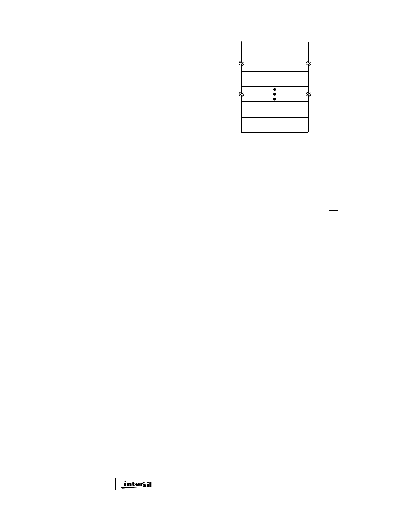
TABLE 10. HS-80C86RH REGISTER MODEL
FIGURE 5. INTERRUPT ACKNOWLEDGE SEQUENCE
Halt
When a software “HALT” instruction is executed the pro- ces-
sor indicates that it is entering the “HALT” state in one of two
ways depending upon which mode is strapped. In minimum
mode, the processor issues one ALE with no qualifying bus
control signals. In maximum mode the processor issues
appropriate HALT status on S2, S1, S0 and the 82C88 bus
controller issues one ALE. The HS-80C86RH will not leave
the “HALT” state when a local bus “hold” is entered while in
“HALT”. In this case, the processor reissues the HALT indi-
cator at the end of the local bus hold. An NMl or interrupt
request (when interrupts enabled) or RESET will force the
HS-80C86RH out of the “HALT” state.
Read/Modify/Write (Semaphore)
Operations Via Lock
The LOCK status information is provided by the processor
when consecutive bus cycles are required during the execu-
tion of an instruction. This gives the processor the capability
of performing read/modify/write operations on memory (via
the Exchange Register With Memory instruction, for exam-
ple) without another system bus master receiving interven-
ing memory cycles. This is useful in multiprocessor system
configurations to accomplish “test and set lock” operations.
The LOCK signal is activated (forced LOW) in the clock cycle
following decoding of the software “LOCK” prefix instruction.
It is deactivated at the end of the last bus cycle of the
instruction following the “LOCK” prefix instruction. While
LOCK is active a request on a RQ/GT pin will be recorded
and then honored at the end of the LOCK.
AX
AH
BX
BH
CX
CH
DX
DH
AL
ACCUMULATOR
BL
BASE
CL
COUNT
DL
DATA
SP
STACK POINTER
BP
BASE POINTER
SI
SOURCE INDEX
DI
DESTINATION INDEX
IP
FLAGSH FLAGSL
INSTRUCTION POINTER
STATUS FLAGS
CS
CODE SEGMENT
DS
DATA SEGMENT
SS
STACK SEGMENT
ES
EXTRA SEGMENT
MULTIBUS™ is an Intel Trademark
System Timing - Minimum System
The read cycle begins in T1 with the assertion of the
Address Latch Enable (ALE) signal. The trailing (low-going)
edge of this signal is used to latch the address information,
which is valid on the address/data bus (AD0-AD15) at this
time, into the 82C82 latches. The BHE and A0 signals
address the low, high or both bytes. From T1 to T4 the M/IO
signal indicates a memory or I/O operation. At T2, the
address is removed from the address/data bus and the bus
is held at the last valid logic state by internal bus hold
devices. The read control signal is also asserted at T2. The
read (RD) signal causes the addressed device to enable its
data bus drivers to the local bus. Some time later, valid data
Spec Number 518055
872
Share Link: 