HD74AC175 데이터 시트보기 (PDF) - Hitachi -> Renesas Electronics
부품명
상세내역
일치하는 목록
HD74AC175 Datasheet PDF : 10 Pages
| |||
HD74AC175
Functional Description
The HD74AC175 consists of four edge-triggered D flip-flops with individual D inputs and Q and Q
outputs. The Clock and Master Reset are common. The four flip-flops will store the state of their
individual D inputs on the Low-to-High clock (CP) transition, causing individual Q and Q outputs to
follow. A Low input on the Master Reset (MR) will force all Q outputs Low and Q outputs High
independent of Clock or Data inputs. The HD74AC175 is useful for general logic applications where a
common Master Reset and Clock are acceptable.
Truth Table
Inputs
Outputs
@ tn, MR = H
@ tn+1
Dn
Qn
Qn
L
L
H
H
H
L
H : High Voltage Level
L : Low Voltage Level
tn : Bit Time before Clock Pulse
tn + 1: Bit Time after Clock Pulse
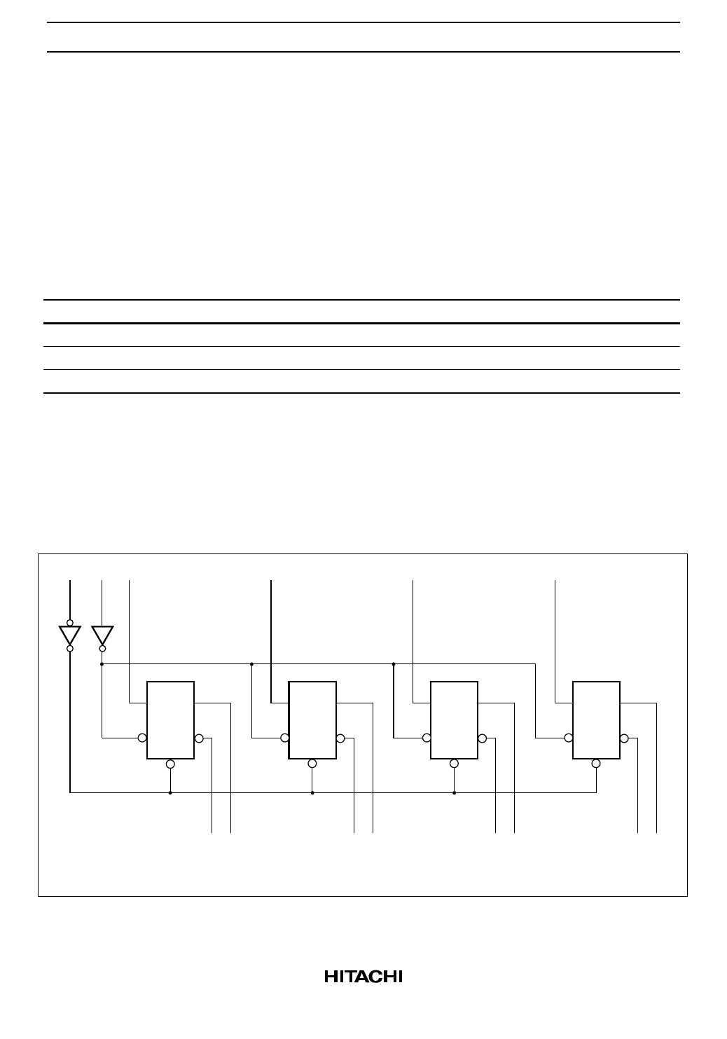
Logic Diagram
MR CP D3
D2
D1
D0
DQ
CP Q
CD
DQ
CP Q
CD
DQ
CP Q
CD
DQ
CP Q
CD
Q3 Q3
Q2 Q2
Q1 Q1
Q0 Q0
Please note that this diagram is provided only for the understanding of logic operations and should not be
used to estimate propagation delays.
3
Share Link: 