MC14042B 데이터 시트보기 (PDF) - Motorola => Freescale
부품명
상세내역
일치하는 목록
MC14042B Datasheet PDF : 6 Pages
| |||
MOTOROLA
SEMICONDUCTOR TECHNICAL DATA
Quad Transparent Latch
The MC14042B Quad Transparent Latch is constructed with MOS
P–channel and N–channel enhancement mode devices in a single
monolithic structure. Each latch has a separate data input, but all four
latches share a common clock. The clock polarity (high or low) used to
strobe data through the latches can be reversed using the polarity input.
Information present at the data input is transferred to outputs Q and Q during
the clock level which is determined by the polarity input. When the polarity
input is in the logic “0” state, data is transferred during the low clock level,
and when the polarity input is in the logic “1” state the transfer occurs during
the high clock level.
• Buffered Data Inputs
• Common Clock
• Clock Polarity Control
• Q and Q Outputs
• Double Diode Input Protection
• Supply Voltage Range = 3.0 Vdc to 1 8 Vdc
ÎÎÎÎÎÎÎÎÎÎÎÎÎÎÎÎÎÎÎÎÎ • Capable of Driving Two Low–power TTL Loads or One Low–power
Schottky TTL Load Over the Rated Temperature Range
ÎÎÎÎÎÎÎÎÎÎÎÎÎÎÎÎÎÎÎÎÎÎÎÎÎÎÎÎÎÎÎÎÎÎÎÎÎÎÎÎÎÎ MAXIMUM RATINGS* (Voltages Referenced to VSS)
ÎÎÎÎÎÎÎÎÎÎÎÎÎÎÎÎÎÎÎÎÎ Symbol
Parameter
Value
Unit
ÎÎÎÎÎÎÎÎÎÎÎÎÎÎÎÎÎÎÎÎÎ VDD DC Supply Voltage
– 0.5 to + 18.0
V
ÎÎÎÎÎÎÎÎÎÎÎÎÎÎÎÎÎÎÎÎÎ Vin, Vout Input or Output Voltage (DC or Transient) – 0.5 to VDD + 0.5 V
ÎÎÎÎÎÎÎÎÎÎÎÎÎÎÎÎÎÎÎÎÎ lin, lout Input or Output Current (DC or Transient),
± 10
mA
per Pin
ÎÎÎÎÎÎÎÎÎÎÎÎÎÎÎÎÎÎÎÎÎ PD Power Dissipation, per Package†
500
mW
ÎÎÎÎÎÎÎÎÎÎÎÎÎÎÎÎÎÎÎÎÎ Tstg Storage Temperature
– 65 to + 150
_C
ÎÎÎÎÎÎÎÎÎÎÎÎÎÎÎÎÎÎÎÎÎ TL
Lead Temperature (8–Second Soldering)
260
_C
ÎÎÎÎÎÎÎÎÎÎÎÎÎÎÎÎÎÎÎÎÎ * Maximum Ratings are those values beyond which damage to the device may occur.
†Temperature Derating:
Plastic “P and D/DW” Packages: – 7.0 mW/_C From 65_C To 125_C
Ceramic “L” Packages: – 12 mW/_C From 100_C To 125_C
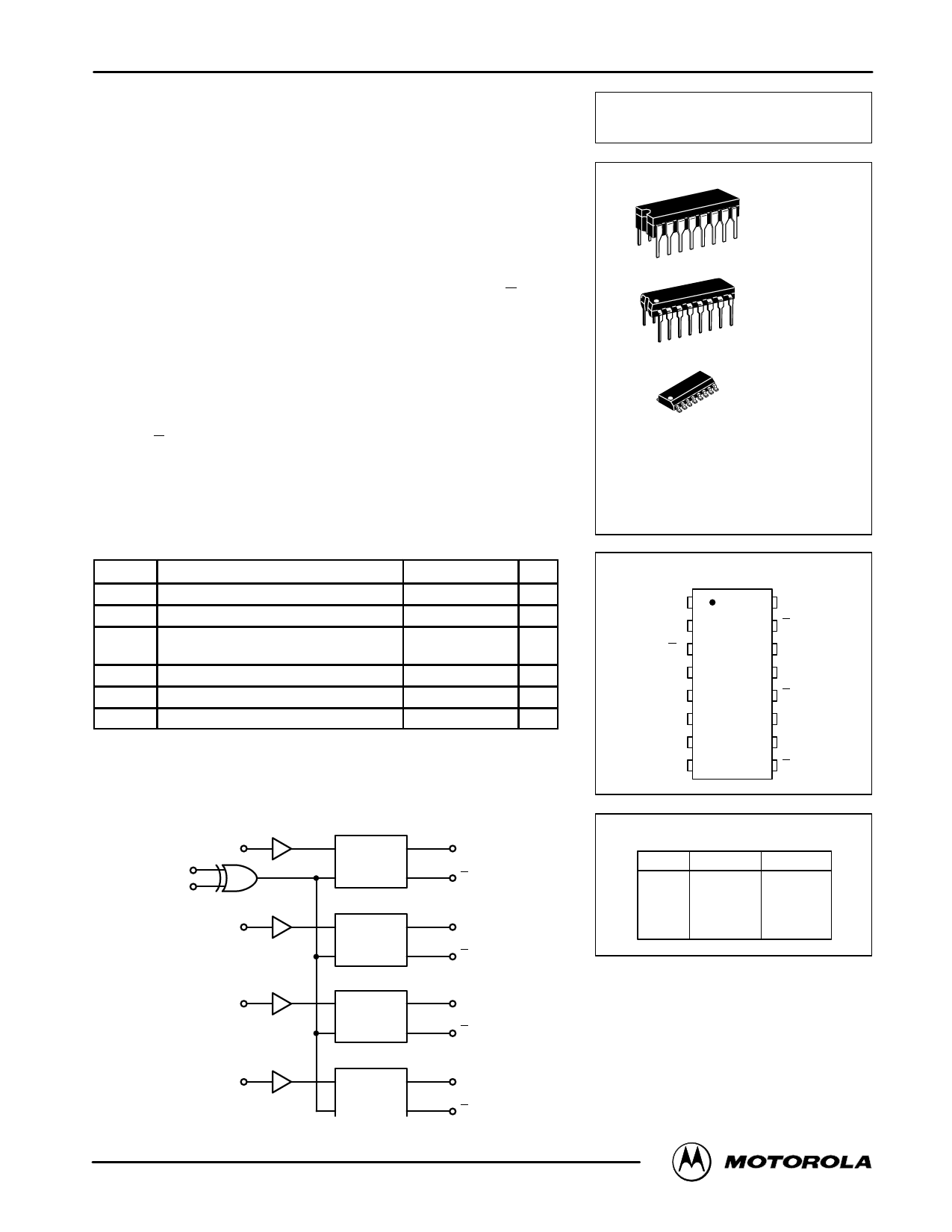
LOGIC DIAGRAM
5
CLOCK
POLARITY
6
D0
4
D1
7
LATCH
1
LATCH
2
Q0
2
Q0
3
Q1
10
Q1
9
D2
13
VDD = PIN 16
VSS = PIN 8
D3
14
REV 3
1/94
©MMCot1or4o0la4, I2nBc. 1995
156
LATCH
3
LATCH
4
Q2
11
Q2
12
Q3
1
Q3
15
MC14042B
L SUFFIX
CERAMIC
CASE 620
P SUFFIX
PLASTIC
CASE 648
D SUFFIX
SOIC
CASE 751B
ORDERING INFORMATION
MC14XXXBCP
MC14XXXBCL
MC14XXXBD
Plastic
Ceramic
SOIC
TA = – 55° to 125°C for all packages.
PIN ASSIGNMENT
Q3 1
Q0 2
Q0 3
D0 4
CLOCK 5
POLARITY 6
D1 7
VSS 8
16 VDD
15 Q3
14 D3
13 D2
12 Q2
11 Q2
10 Q1
9 Q1
TRUTH TABLE
Clock
0
1
1
0
Polarity
0
0
1
1
Q
Data
Latch
Data
Latch
MOTOROLA CMOS LOGIC DATA
Share Link: 