74HC125D(2015) 데이터 시트보기 (PDF) - NXP Semiconductors.
부품명
상세내역
일치하는 목록
74HC125D Datasheet PDF : 16 Pages
| |||
Nexperia
74HC125; 74HCT125
Quad buffer/line driver; 3-state
Table 7. Dynamic characteristics …continued
Voltages are referenced to GND (ground = 0 V); CL = 50 pF unless otherwise specified; for test circuit see Figure 7.
Symbol Parameter Conditions
25 C
40 C to +85 C 40 C to +125 C Unit
Min Typ Max Min Max
Min
Max
74HCT125
tpd
propagation nA to nY; see Figure 5
[1]
delay
VCC = 4.5 V
-
15 25
-
31
-
38 ns
VCC = 5 V; CL = 15 pF
-
12
-
-
-
-
-
ns
ten
enable time nOE to nY; see Figure 6 [2]
VCC = 4.5 V
-
15 28
-
35
-
42 ns
tdis
disable time nOE to nY; see Figure 6 [3]
VCC = 4.5 V
-
15 25
-
31
-
38 ns
tt
transition nY; see Figure 5
time
[4] -
5 12
-
15
-
18 ns
CPD
power
CL = 50 pF; f = 1 MHz;
[5] -
24 -
-
-
-
-
pF
dissipation VI = GND to VCC 1.5 V
capacitance
[1] tpd is the same as tPLH and tPHL.
[2] ten is the same as tPZH and tPZL.
[3] tdis is the same as tPLZ and tPHZ.
[4] tt is the same as tTHL and tTLH.
[5] CPD is used to determine the dynamic power dissipation (PD in W).
PD = CPD VCC2 fi N + (CL VCC2 fo) where:
fi = input frequency in MHz;
fo = output frequency in MHz;
CL = output load capacitance in pF;
VCC = supply voltage in V;
N = number of inputs switching;
(CL VCC2 fo) = sum of outputs.
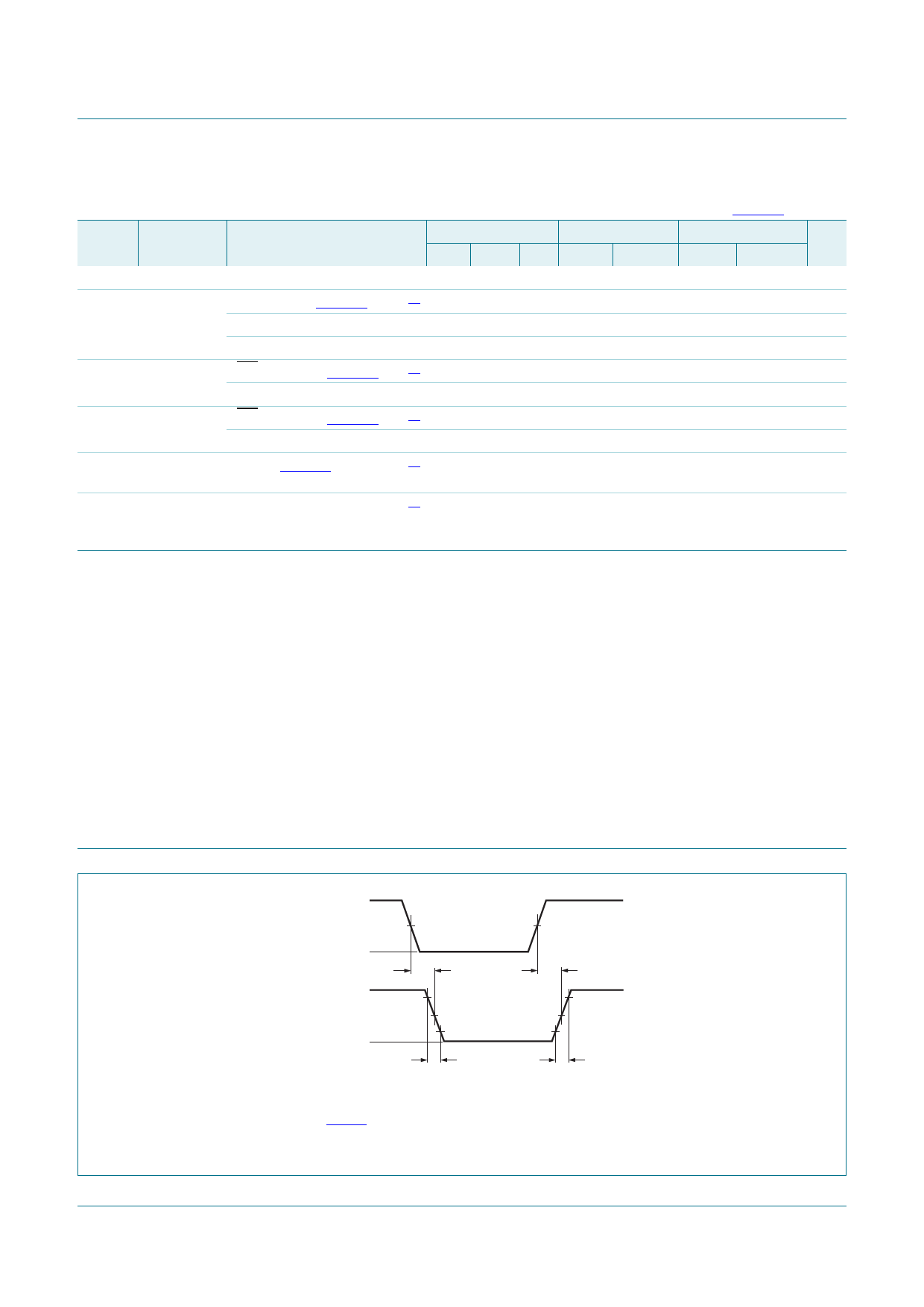
11. Waveforms
9,
Q$LQSXW
*1'
92+
Q<RXWSXW
92/
90
W3+/
90
W7+/
90
90
W3/+
W7/+
DDD
Fig 5.
Measurement points are given in Table 8.
VOL and VOH are typical voltage output levels that occur with the output load.
Propagation delay input (nA) to output (nY)
74HC_HCT125
Product data sheet
All information provided in this document is subject to legal disclaimers.
Rev. 6 — 1 December 2015
© Nexperia B.V. 2017. All rights reserved
7 of 16
Share Link: 