SL4066BN 데이터 시트보기 (PDF) - System Logic Semiconductor
부품명
상세내역
일치하는 목록
SL4066BN Datasheet PDF : 6 Pages
| |||
SL4066B
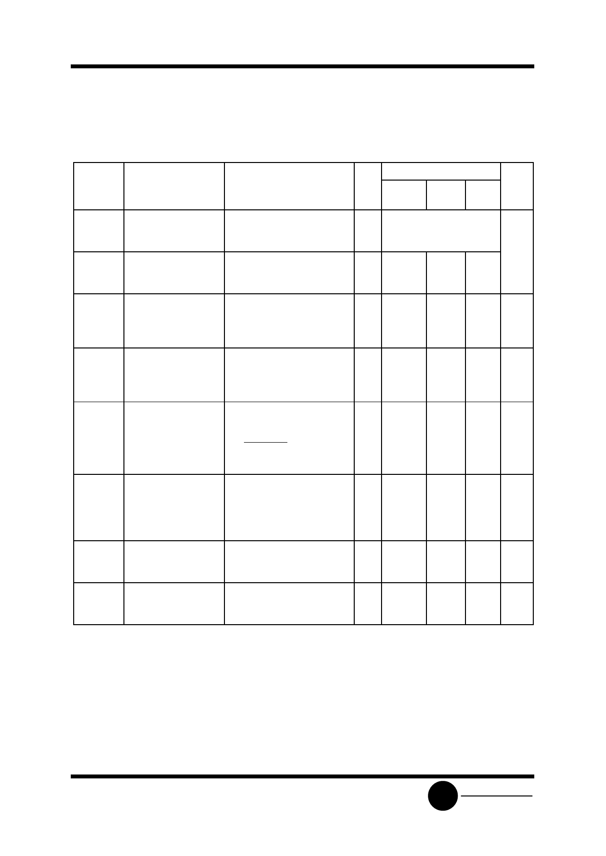
DC ELECTRICAL CHARACTERISTICS(Voltages Referenced to GND)
Symbol
Parameter
Test Conditions
VIH Minimum High-Level RON= Per Spec
Voltage ON/Off
Control Inputs
VIL
Minimum Low-Level RON = Per Spec
Voltage ON/Off
Control Inputs
IIN
Maximum Input
Leakage Current,
ON/OFF Control
Inputs
VIN = VCC or GND
ICC
Maximum Quiescent VIN = VCC or GND
Supply Current
(per Package)
RON
∆RON
IOFF
ION
Maximum “ON”
Resistance
VC= VCC
RL=10 kΩ returned
to VCC - GND
2
VIS= GND to VCC
Maximum Difference
in “ON” Resistance
Between Any Two
Channels in the Same
Package
VC= VCC
RL=10 kΩ
Maximum Off-Channel VC= 0 V
Leakage Current, Any VIS=18 V; VOS= 0 V
One Channel
VIS=0 V; VOS= 18V
Maximum On-Channel VC= 0 V
Leakage Current, Any VIS=18 V; VOS= 0 V
One Channel
VIS=0 V; VOS= 18V
VCC
Guaranteed Limit
V ≥-55°C 25 ≤125 Unit
°C
°C
5.0
3.5(Min)
V
10
7(Min)
15
11(Min)
5.0
1
10
2
15
2
1
1
V
2
2
2
2
18 ±0.1
±0.1 ±1.0 µA
5.0 0.25
10 0.5
15
1
20
5
5.0 800
10 310
15 200
0.25 7.5 µA
0.5
15
1
30
5
150
1050 1300 Ω
400 550
240 320
5.0
-
10
-
15
-
15
-
Ω
10
-
5
-
18 ±0.1
±0.1 ±1.0 µA
18 ±0.1
±0.1 ±1.0 µA
SLS
System Logic
Semiconductor
Share Link: 