MC74HC4016AD 데이터 시트보기 (PDF) - Motorola => Freescale
부품명
상세내역
일치하는 목록
MC74HC4016AD Datasheet PDF : 12 Pages
| |||
MOTOROLA
SEMICONDUCTOR TECHNICAL DATA
Product Preview
MC54/74HC4016A
Quad Analog Switch/
Multiplexer/Demultiplexer
High–Performance Silicon–Gate CMOS
The MC54/74HC4016A utilizes silicon–gate CMOS technology to
achieve fast propagation delays, low ON resistances, and low OFF–
channel leakage current. This bilateral switch/multiplexer/demultiplexer
controls analog and digital voltages that may vary across the full
power–supply range (from VCC to GND).
The HC4016A is identical in pinout to the metal–gate CMOS MC14016
and MC14066. Each device has four independent switches. The device
has been designed so that the ON resistances (RON) are much more
linear over input voltage than RON of metal–gate CMOS analog switches.
This device is identical in both function and pinout to the HC4066A. The
ON/OFF Control inputs are compatible with standard CMOS outputs; with
pullup resistors, they are compatible with LSTTL outputs. For analog
switches with voltage–level translators, see the HC4316A. For analog
switches with lower RON characteristics, use the HC4066A.
• Fast Switching and Propagation Speeds
• High ON/OFF Output Voltage Ratio
• Low Crosstalk Between Switches
• Diode Protection on All Inputs/Outputs
• Wide Power–Supply Voltage Range (VCC – GND) = 2.0 to 12.0 Volts
• Analog Input Voltage Range (VCC – GND) = 2.0 to 12.0 Volts
• Improved Linearity and Lower ON Resistance over Input Voltage than
the MC14016 or MC14066
• Low Noise
• Chip Complexity: 32 FETs or 8 Equivalent Gates
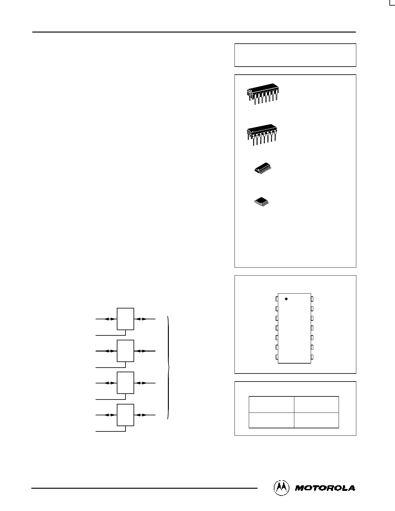
14
1
J SUFFIX
CERAMIC PACKAGE
CASE 632–08
14
1
14
1
N SUFFIX
PLASTIC PACKAGE
CASE 646–06
D SUFFIX
SOIC PACKAGE
CASE 751A–03
14
1
DT SUFFIX
TSSOP PACKAGE
CASE 948G–01
ORDERING INFORMATION
MC54HCXXXXAJ
MC74HCXXXXAN
MC74HCXXXXAD
MC74HCXXXXADT
Ceramic
Plastic
SOIC
TSSOP
PIN ASSIGNMENT
LOGIC DIAGRAM
XA 1
A ON/OFF CONTROL 13
2 YA
XB 4
3 YB
B ON/OFF CONTROL 5
XC 8
C ON/OFF CONTROL 6
9 YC
ANALOG
OUTPUTS/INPUTS
XD 11
10 YD
D ON/OFF CONTROL 12
ANALOG INPUTS/OUTPUTS = XA, XB, XC, XD
PIN 14 = VCC
PIN 7 = GND
XA 1
YA 2
YB 3
XB 4
B ON/OFF
CONTROL
5
C ON/OFF 6
CONTROL
GND 7
14 VCC
13
A ON/OFF
CONTROL
12 D ON/OFF
CONTROL
11 XD
10 YD
9 YC
8 XC
FUNCTION TABLE
On/Off Control
Input
L
H
State of
Analog Switch
Off
On
This document contains information on a product under development. Motorola reserves the right to change or discontinue this product without notice.
10/95
© Motorola, Inc. 1995
3–1
REV 0
Share Link: 