AD8024AR 데이터 시트보기 (PDF) - Analog Devices
부품명
상세내역
일치하는 목록
AD8024AR Datasheet PDF : 12 Pages
| |||
AD8024
Overload Recovery
The most important overload conditions are:
Input Common-Mode Voltage Overdrive
Output Voltage Overdrive
Input Current Overdrive.
When configured for a low closed-loop gain, the AD8024
recovers quickly from an input common-mode voltage over-
drive; typically in <25 ns.
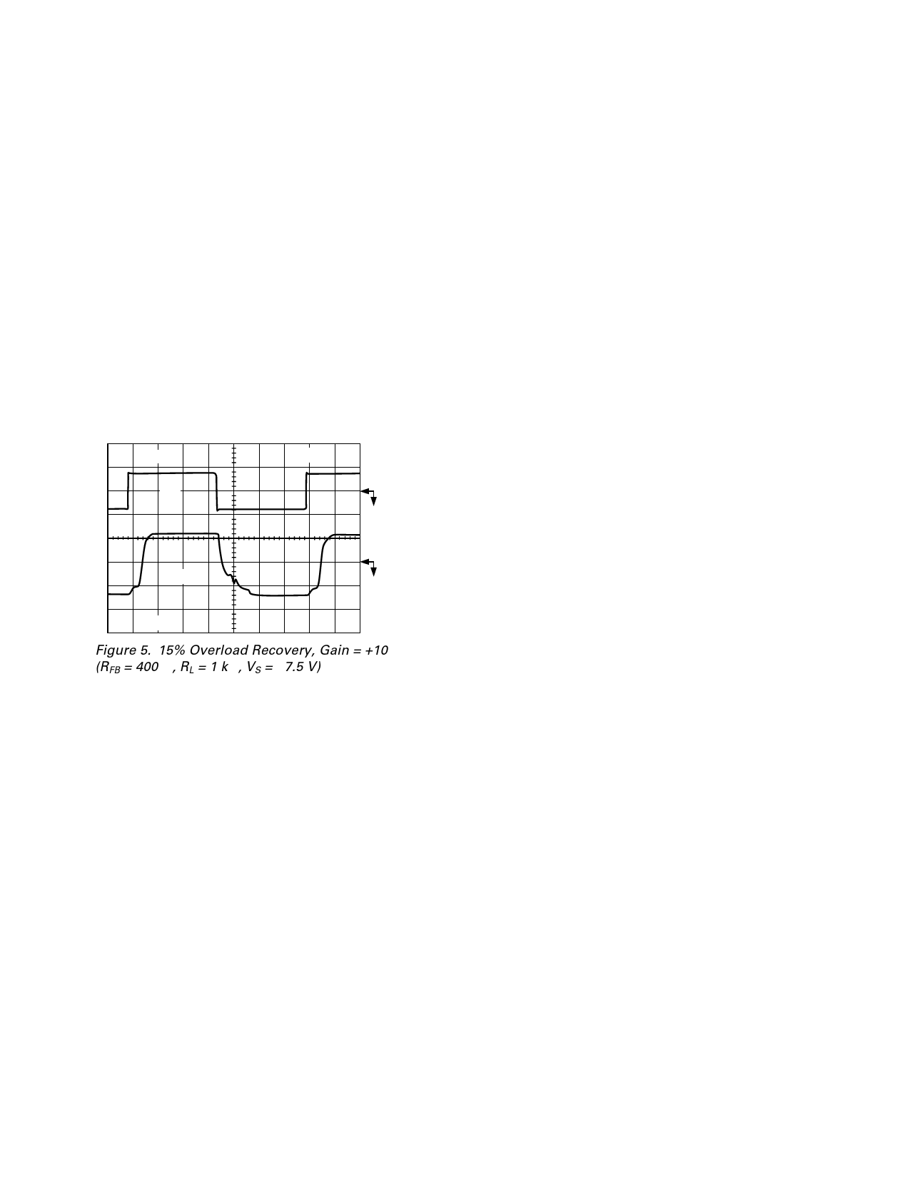
When configured for a higher gain and overloaded at the output,
recovery from an output voltage overdrive is also short; approxi-
mately 55 ns (see Figure 5). For higher overdrive, the response
is somewhat slower. For 100% overdrive, the recovery time is
substantially longer.
When configured for a high noninverting gain, a high input over-
drive can result in a large current into the input stage. Although
this current is internally limited to approximately 30 mA, its
effect on the total power dissipation may be significant. See also
the warning under Maximum Power Dissipation.
Disable Mode Operation
When the Disable pin is tied to DGND, all amplifiers are opera-
tional, in the enabled state.
When the voltage on the Disable pin is raised to 1.6 V or more
above DGND, all amplifiers are in the disabled, powered-down
state. In this condition, the DISABLE pin sources approximately
0.1 µA, the total quiescent current is reduced to approximately
500 µA, all outputs are in a high impedance state, and there is a
high level of isolation from inputs to outputs.
The output impedance in the disabled mode is the equivalent of all
external resistors, seen from the output pin, in parallel with the
total disabled output impedance of the amplifier, typically 20 pF.
The input stages of the AD8024 include protection from large
differential input voltages that may be present in the disabled
mode. Internal clamps limit this voltage to 1.5 V. The high input-
to-output isolation is maintained for voltages below this limit.
1V
VIN
50ns
VOUT
5V
Figure 5. 15% Overload Recovery, Gain = +10
(RFB = 400 Ω, RL = 1 kΩ, VS = ±7.5 V)
–10–
REV. C
Share Link: 