MC74HCT32A 데이터 시트보기 (PDF) - Motorola => Freescale
부품명
상세내역
일치하는 목록
MC74HCT32A Datasheet PDF : 5 Pages
| |||
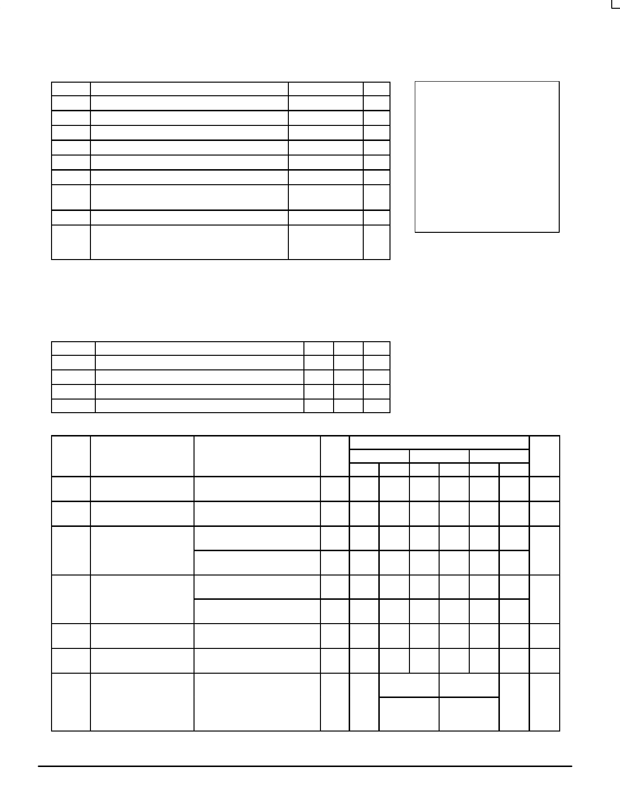
ÎÎÎÎÎÎÎÎÎÎÎÎÎÎÎÎÎÎÎÎÎÎÎ MC54/74HCT32A
ÎÎÎÎÎÎÎÎÎÎÎÎÎÎÎÎÎÎÎÎÎÎÎÎÎÎÎÎÎÎÎÎÎÎÎÎÎÎÎÎÎÎÎÎÎÎ MAXIMUM RATINGS*
ÎÎÎÎÎÎÎÎÎÎÎÎÎÎÎÎÎÎÎÎÎÎÎ Symbol
Parameter
Value
Unit
ÎÎÎÎÎÎÎÎÎÎÎÎÎÎÎÎÎÎÎÎÎÎÎ VCC
ÎÎÎÎÎÎÎÎÎÎÎÎÎÎÎÎÎÎÎÎÎÎÎ Vin
ÎÎÎÎÎÎÎÎÎÎÎÎÎÎÎÎÎÎÎÎÎÎÎ Vout
ÎÎÎÎÎÎÎÎÎÎÎÎÎÎÎÎÎÎÎÎÎÎÎ Iin
ÎÎÎÎÎÎÎÎÎÎÎÎÎÎÎÎÎÎÎÎÎÎÎ Iout
ÎÎÎÎÎÎÎÎÎÎÎÎÎÎÎÎÎÎÎÎÎÎÎ ICC
ÎÎÎÎÎÎÎÎÎÎÎÎÎÎÎÎÎÎÎÎÎÎÎ PD
DC Supply Voltage (Referenced to GND)
– 0.5 to + 7.0
V
DC Input Voltage (Referenced to GND)
DC Output Voltage (Referenced to GND)
DC Input Current, per Pin
– 1.5 to VCC + 1.5 V
– 0.5 to VCC + 0.5 V
± 20
mA
DC Output Current, per Pin
± 25
mA
DC Supply Current, VCC and GND Pins
± 50
mA
Power Dissipation in Still Air, Plastic or Ceramic DIP†
750
mW
SOIC Package†
500
ÎÎÎÎÎÎÎÎÎÎÎÎÎÎÎÎÎÎÎÎÎÎÎ Tstg Storage Temperature
– 65 to + 150
_C
ÎÎÎÎÎÎÎÎÎÎÎÎÎÎÎÎÎÎÎÎÎÎÎ TL Lead Temperature, 1 mm from Case for 10 Seconds
_C
ÎÎÎÎÎÎÎÎÎÎÎÎÎÎÎÎÎÎÎÎÎÎÎ (Plastic DIP)
260
_C
(Ceramic DIP)
300
ÎÎÎÎÎÎÎÎÎÎÎÎÎÎÎÎÎÎÎÎÎÎÎÎÎÎÎÎÎÎÎÎÎÎÎÎÎÎÎÎÎÎÎÎÎÎ *Maximum Ratings are those values beyond which damage to the device may occur.
This device contains protection
circuitry to guard against damage
due to high static voltages or electric
fields. However, precautions must
be taken to avoid applications of any
voltage higher than maximum rated
voltages to this high–impedance cir-
cuit. For proper operation, Vin and
v v Vout should be constrained to the
range GND (Vin or Vout) VCC.
Unused inputs must always be
tied to an appropriate logic voltage
level (e.g., either GND or VCC).
Unused outputs must be left open.
Functional operation should be restricted to the Recommended Operating Conditions.
†Derating — Plastic DIP: – 10 mW/_C from 65_ to 125_C
Ceramic DIP: – 10 mW/_C from 100_ to 125_C
SOIC Package: – 7 mW/_C from 65_ to 125_C
ÎÎÎÎÎÎÎÎÎÎÎÎÎÎÎÎÎÎÎÎÎÎÎ For high frequency or heavy load considerations, see Chapter 2 of the Motorola High–Speed CMOS Data Book (DL129/D).
ÎÎÎÎÎÎÎÎÎÎÎÎÎÎÎÎÎÎÎÎÎÎÎ RECOMMENDED OPERATING CONDITIONS
ÎÎÎÎÎÎÎÎÎÎÎÎÎÎÎÎÎÎÎÎÎÎÎ Symbol
ÎÎÎÎÎÎÎÎÎÎÎÎÎÎÎÎÎÎÎÎÎÎÎ VCC
ÎÎÎÎÎÎÎÎÎÎÎÎÎÎÎÎÎÎÎÎÎÎÎ Vin, Vout
TA
ÎÎÎÎÎÎÎÎÎÎÎÎÎÎÎÎÎÎÎÎÎÎÎÎÎÎÎÎÎÎÎÎÎ tr, tf
Parameter
DC Supply Voltage (Referenced to GND)
DC Input Voltage, Output Voltage (Referenced to GND)
Operating Temperature, All Package Types
Input Rise and Fall Time (Figure 1)
Min Max Unit
4.5 5.5 V
0 VCC V
– 55 + 125 _C
0 500 ns
ÎÎÎÎÎÎÎÎÎÎÎÎÎÎÎÎÎÎÎÎÎÎÎÎÎÎÎÎÎÎÎÎÎÎÎÎÎÎÎÎÎÎÎÎÎÎÎÎÎÎÎÎÎÎÎÎÎÎÎÎÎÎÎÎÎÎ DC ELECTRICAL CHARACTERISTICS FOR THE MC54/74HCT32A (Voltages Referenced to GND)
ÎÎÎÎÎÎÎÎÎÎÎÎÎÎÎÎÎÎÎÎÎÎÎÎÎÎÎÎÎÎÎÎÎÎÎÎÎÎÎÎÎÎÎÎÎÎÎÎÎÎÎÎÎÎÎÎÎÎÎÎÎÎÎÎÎÎ Symbol
Parameter
Test Conditions
Guaranteed Limits
VCC – 55 to 25_C
v 85_C
v 125_C
Volts Min Max Min Max Min Max Unit
ÎÎÎÎÎÎÎÎÎÎÎÎÎÎÎÎÎÎÎÎÎÎÎÎÎÎÎÎÎÎÎÎÎ VIH Minimum High–Level
ÎÎÎÎÎÎÎÎÎÎÎÎÎÎÎÎÎÎÎÎÎÎÎÎÎÎÎÎÎÎÎÎÎ Input Voltage
v Vout = 0.1 V or VCC – 0.1 V
|Iout| 20 µA
4.5 2.0
5.5 2.0
2.0
2.0
2.0
2.0
V
ÎÎÎÎÎÎÎÎÎÎÎÎÎÎÎÎÎÎÎÎÎÎÎÎÎÎÎÎÎÎÎÎÎ VIL
ÎÎÎÎÎÎÎÎÎÎÎÎÎÎÎÎÎÎÎÎÎÎÎÎÎÎÎÎÎÎÎÎÎÎÎÎÎÎÎÎÎÎÎÎÎÎÎÎÎÎÎÎÎÎÎÎÎÎÎÎÎÎÎÎÎÎ VOH
ÎÎÎÎÎÎÎÎÎÎÎÎÎÎÎÎÎÎÎÎÎÎÎÎÎÎÎÎÎÎÎÎÎÎÎÎÎÎÎÎÎÎÎÎÎÎÎÎÎÎÎÎÎÎÎÎÎÎÎÎÎÎÎÎÎÎÎÎÎÎÎÎÎÎÎÎÎÎÎÎÎÎÎÎÎÎÎÎÎÎÎÎÎÎÎÎÎÎÎ VOL
ÎÎÎÎÎÎÎÎÎÎÎÎÎÎÎÎÎÎÎÎÎÎÎÎÎÎÎÎÎÎÎÎÎÎÎÎÎÎÎÎÎÎÎÎÎÎÎÎÎÎÎÎÎÎÎÎÎÎÎÎÎÎÎÎÎÎÎÎÎÎÎÎÎÎÎÎÎÎÎÎÎÎÎÎÎÎÎÎÎÎÎÎÎÎÎÎÎÎÎ Iin
Maximum Low–Level
Input Voltage
Minimum High–Level
Output Voltage
Maximum Low–Level
Output Voltage
Maximum Input Leakage
Current
v Vout = 0.1 V or VCC – 0.1 V
|Iout| 20 µA
v Vin = VIH or VIL
|Iout| 20 µA
v Vin = VIH or VIL
|Iout| 4.0 mA
v Vin = VIH or VIL
|Iout| 20 µA
v Vin = VIH or VIL
|Iout| 4.0 mA
Vin = VCC or GND
4.5
0.8
0.8
0.8
V
5.5
0.8
0.8
0.8
4.5 4.4
4.4
4.4
V
5.5 5.4
5.4
5.4
5.5 3.98
3.84
3.7
4.5
0.1
0.1
0.1
V
5.5
0.1
0.1
0.1
4.5
0.26
0.33
0.4
5.5
± 0.1
± 1.0
± 1.0 µA
ÎÎÎÎÎÎÎÎÎÎÎÎÎÎÎÎÎÎÎÎÎÎÎÎÎÎÎÎÎÎÎÎÎ ICC Maximum Quiescent Sup- Vin = VCC or GND
ÎÎÎÎÎÎÎÎÎÎÎÎÎÎÎÎÎÎÎÎÎÎÎÎÎÎÎÎÎÎÎÎÎ ply Current (per Package) Iout = 0 µA
5.5
1.0
10
40
µA
ÎÎÎÎÎÎÎÎÎÎÎÎÎÎÎÎÎÎÎÎÎÎÎÎÎÎÎÎÎÎÎÎÎÎÎÎÎÎÎÎÎÎÎÎÎÎÎÎÎÎÎÎÎÎÎÎÎÎÎÎÎÎÎÎÎÎ ≥ – 55_C
25_C to
125_C
ÎÎÎÎÎÎÎÎÎÎÎÎÎÎÎÎÎÎÎÎÎÎÎÎÎÎÎÎÎÎÎÎÎ ∆ICC Additional Quiescent
Vin = 2.4 V, Any One Input
5.5
2.9
2.4
mA
Supply Current
Vin = VCC or GND, Other Inputs
ÎÎÎÎÎÎÎÎÎÎÎÎÎÎÎÎÎÎÎÎÎÎÎÎÎÎÎÎÎÎÎÎÎ lout = 0 µA
ÎÎÎÎÎÎÎÎÎÎÎÎÎÎÎÎÎÎÎÎÎÎÎÎÎÎÎÎÎÎÎÎÎ NOTE: Information on typical parametric values can be found in Chapter 2 of the Motorola High–Speed CMOS Data Book (DL129/D).
MOTOROLA
2
High–Speed CMOS Logic Data
DL129 — Rev 6
Share Link: 