SL4029BDW 데이터 시트보기 (PDF) - System Logic Semiconductor
부품명
상세내역
일치하는 목록
SL4029BDW Datasheet PDF : 8 Pages
| |||
SL4029B
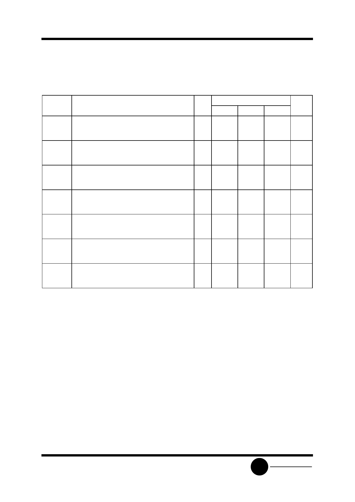
TIMING REQUIREMENTS(CL=50pF, RL=200 kΩ, Input tr=tf=20 ns)
Symbol
Parameter
VCC
Guaranteed Limit
V ≥-55°C 25°C ≤125°C Unit
tw
Minimum Pulse Width, Clock (Figure 1)
5.0 180
180
360
ns
10
90
90
180
15
60
60
120
tw
Minimum Pulse Width, Preset Enable
(Figure 1)
tsu*
Minimum Setup Time, Clock to B/D or U/D
(Figure 1)
5.0 130
130
260
ns
10
70
70
140
15
50
50
100
5.0 340
340
680
ns
10
140
140
280
15
100
100
200
trem* Minimum Removal Time, Preset Enable (Figure 1) 5.0
200
200
400
ns
10
110
110
220
15
80
80
160
th**
Minimum Hold Time, Clock to Carry In (Figure 2) 5.0
50
50
100
ns
10
30
30
60
15
25
25
50
tsu
Minimum Setup Time, Carry In to Clock (Figure 5.0
200
200
400
ns
1)
10
70
70
140
15
60
60
120
tr, tf**
Maximum Input Rise and Fall Times,Clock
(Figure 2)
5.0
15
15
30
µs
10
15
15
30
15
15
15
30
* From Up/Down, Binary/Decode, Carry In, or Preset Enable Control Inputs to Clock Edge.
** From Carry In to Clock Edge
SLS
System Logic
Semiconductor
Share Link: 