NJU6624AFG1 데이터 시트보기 (PDF) - Japan Radio Corporation
부품명
상세내역
일치하는 목록
NJU6624AFG1
Japan Radio Corporation

NJU6624AFG1 Datasheet PDF : 35 Pages
| |||
NJU6624A/B
(4)Instructions
The NJU6624A/B incorporates two registers, an Instruction Register (IR) and a Data Register(DR).
These two registers store control information temporarily to allow interface between NJU6624A/B and MPU or
peripheral ICs operating different cycles.
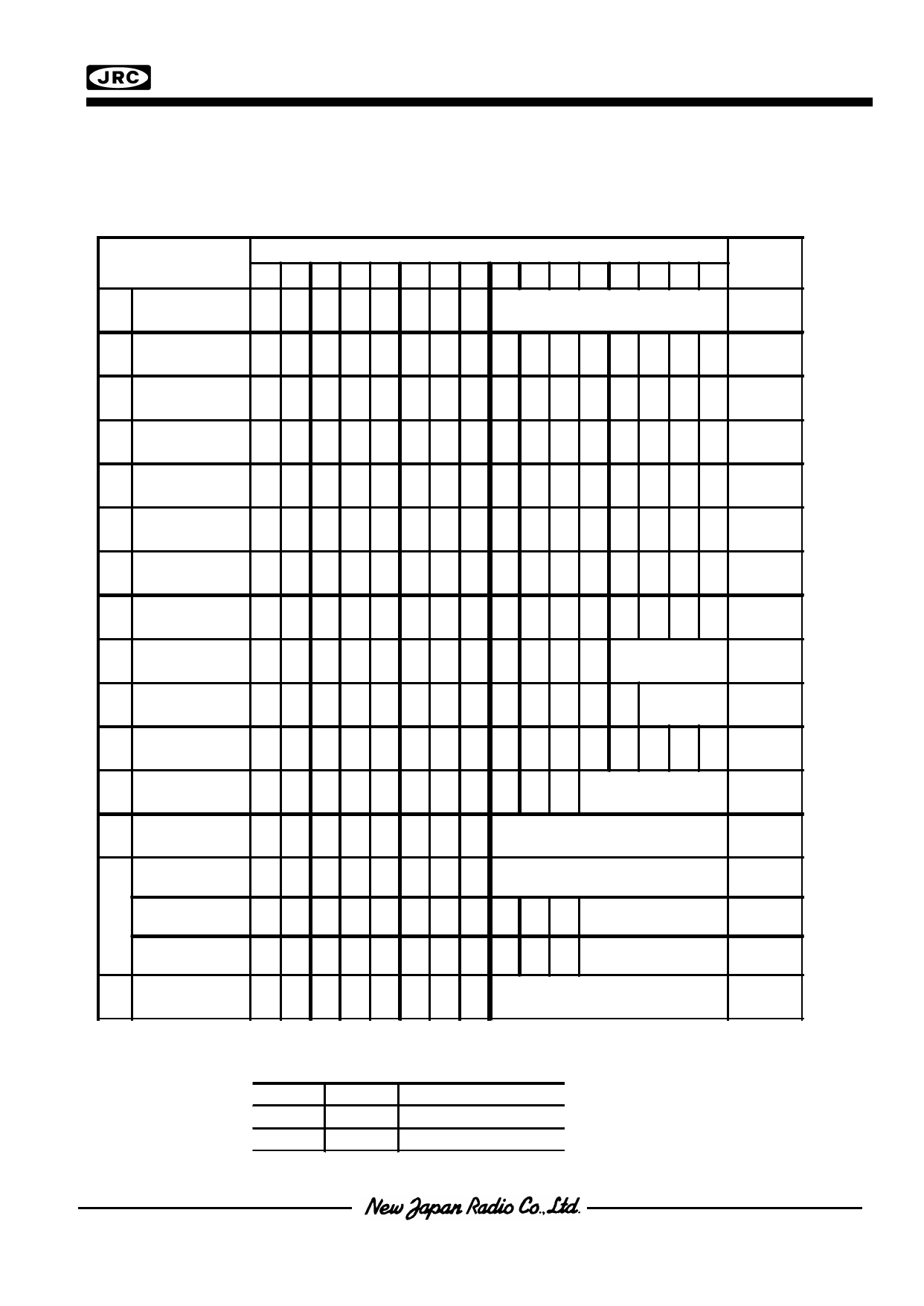
INSTRUCTION
Table 4. Table of Instructions
CODE
Execute
D15 D14 D13 D12 D11 D10 D9 D8 D7 D6 D5 D4 D3 D2 D1 D0 Time
(a) Maker Testing
MS1 MS0 0 1 1 1 1 1
Test data
-
(b) Clear Display
MS1 MS0 0 1 1 0 0 1 * * * * * * * * 234.48uS
(c) Return Home
MS1 MS0 0 1 0 0 0 1 * * * * * * * *
0uS
(d) Entry Mode Set MS1 MS0 0 0 1 0 0 0 * * * * * * I/D S
0uS
(e)
Display ON/OFF
Control
MS1 MS0 0
0
10
0
1*
*
*
*
*
DMB
0uS
(f) Address Shift
MS1 MS0 0 1 0 0 1 0 * * * * * * * ARL 0uS
(g) Display Shift
MS1 MS0 0 0 1 0 1 0 * * * * * * * DRL 0uS
(h) Set Static Port MS1 MS0 0 0 1 0 1 1 * * * * P3 P2 P1 P0 0uS
(i) Contrast Control MS1 MS0 0 0 1 1 0 0 * * * * E.V.R. Value
0uS
(j) Dot Shift
MS1 MS0 0 0 1 1 0 1 *
(k)
Set Display
Mode
MS1 MS0 0
0
11
1
0
*
(l)
Set DD/MK RAM
Address
MS1 MS0
0
1
0
0
1
1
*
(m)
Set CG RAM
Address
MS1 MS0 0
1
0
0
0
0
Write DD RAM
Data
MS1 MS0 0
1
10
0
0
(n)
Write MK RAM
Data
MS1 MS0 0
1
10
0
0
*
Write CG RAM
Data
MS1 MS0 0
1
10
0
0
*
(o)
Read Keyscan
Data
MS1 MS0 1
0
0
1
1
1
*
*
*
*
Number of
Dot Shift
0uS
* * * * * K PD 0uS
*
*
DD RAM(00 to 0D)H
MK RAM(10 to 1B)H
0uS
CG RAM(00 to FE)H
0uS
Write data(DD RAM)
41.38uS
* * Write data(MK RAM) 41.38uS
* * Write data(CGRAM) 41.38uS
Key Data
0uS
MS1,MS0 : Discriminate master or slave. And write code (meet code for selected device) like as mentioned
below.
MS1
1
0
MS0
0
1
DEVICE
NJU6624A
NJU6624B
Note : fOSC=145KHz. If the oscillation frequency is changed, the execution time is also changed.
Share Link: