MB3802 데이터 시트보기 (PDF) - Fujitsu
부품명
상세내역
일치하는 목록
MB3802 Datasheet PDF : 15 Pages
| |||
MB3802
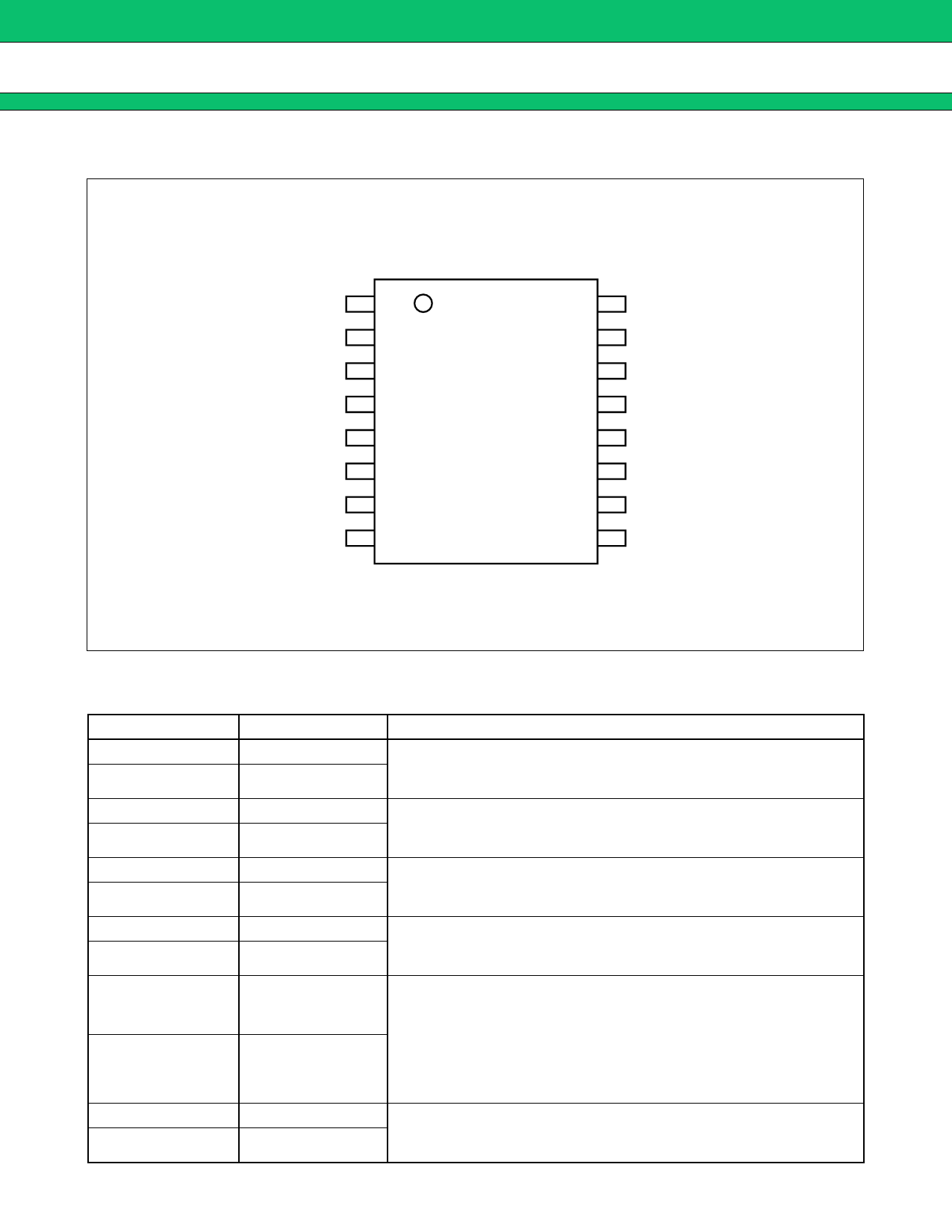
s PIN ASSIGNMENT
GNDA
1
DCGA
2
SWINA
3
SWINA
4
SWINB
5
SWINB
6
DCGB
7
GNDB
8
(TOP VIEW)
MB3802
(FPT-16P-M04)
16
VINA
15
DLYA
14
SWOUTA
13
SWOUTA
12
SWOUTB
11
SWOUTB
10
DLYB
9
VINB
s PIN DESCRIPTION (SCSI Interface)
Pin No.
16
9
3, 4
5, 6
13, 14
11, 12
2
7
15
10
1
8
2
Pin symbol
VINA
VINB
SWINA
SWINB
SWOUTA
SWOUTB
DCGA
DCGB
DLYA
DLYB
GNDA
GNDB
Description
These pins switch ON at High level and OFF at Low level. They
serve as power-supply pins for the DC/DC converter to generate
the switch gate voltage.
Switch Input pins: Two common pins are assigned to SWINA and
SWINB. They serve as power-supply pins for the switch-OFF circuit
which starts at 1.5V min.
Switch output pins: Two common pins are assigned to SWOUTA
and SWOUTB. When DCGA and DCGB are High level, the load-
discharge circuit starts discharge via these pins.
SWOUTA/SWOUTB-side discharge control pins: These pins are
used to discharge from the load-side capacitor at switch OFF.
Connect them to GND when discharge is not required.
Switch-ON/OFF control pins: The ON/OFF time can be delayed
by connecting an external capacitor. Both times are delayed about
three fold by installing a 500-pF capacitor between these pins and
GND. Leave these pins open when they are not used. 10V may be
generated when these pins are open. To keep these pins at high
impedance, take care to mount the device so that no current leaks
(less than 0.1 µA).
Ground pins for input threshold reference voltage and load
discharge: When two switching circuits are used, ground both
GND pins.
Share Link: 