LM323 데이터 시트보기 (PDF) - Motorola => Freescale
부품명
상세내역
일치하는 목록
LM323 Datasheet PDF : 8 Pages
| |||
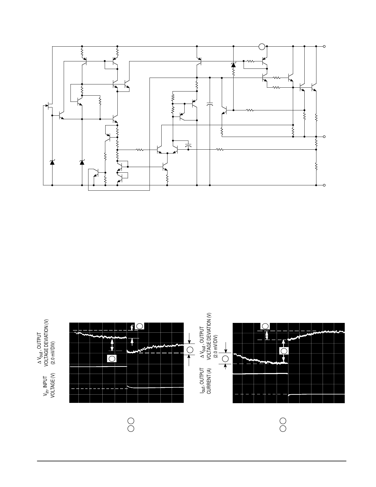
LM323, A
Representative Schematic Diagram
1.0k
Q1
1.0k
Q2
Q4
Q5
Q8
Q9
300
Q3
10k
Q10
Q20
1.0k
2
210
Q22
6.7V 16k
Q21
100
Q24 200
3.0k
10pF
Q19
300
5.6k
Q23
Q16
Input
Q25
Q27
Q26
13 0.12
520
Q12
2.6k 6.0k
40pF
2.0k 3.9k
Q6
Q7
Q13
Q11
6.0k Q14
Q17 Q18
Q15
2.8k
50
7.2k
200
Output
840
1.7k
Gnd
VOLTAGE REGULATOR PERFORMANCE
The performance of a voltage regulator is specified by its
immunity to changes in load, input voltage, power dissipation,
and temperature. Line and load regulation are tested with a
pulse of short duration (< 100 µs) and are strictly a function of
electrical gain. However, pulse widths of longer duration
(> 1.0 ms) are sufficient to affect temperature gradients
across the die. These temperature gradients can cause a
change in the output voltage, in addition to changes by line
and load regulation. Longer pulse widths and thermal
gradients make it desirable to specify thermal regulation.
Thermal regulation is defined as the change in output
voltage caused by a change in dissipated power for a
specified time, and is expressed as a percentage output
voltage change per watt. The change in dissipated power can
be caused by a change in either input voltage or the load
current. Thermal regulation is a function of IC layout and die
attach techniques, and usually occurs within 10 ms of a
change in power dissipation. After 10 ms, additional changes
in the output voltage are due to the temperature coefficient of
the device.
Figure 1 shows the line and thermal regulation response of
a typical LM323A to a 20 W input pulse. The variation of the
output voltage due to line regulation is labeled À and the
thermal regulation component is labeled Á. Figure 2 shows
the load and thermal regulation response of a typical LM323A
to a 20 W load pulse. The output voltage variation due to load
regulation is labeled À and the thermal regulation component
is labeled Á.
Figure 1. Line and Thermal Regulation
2
Figure 2. Load and Thermal Regulation
2
2
1
18 V
8.0 V
t, TIME (2.0 ms/DIV)
Vout = 5.0 V
Vin = 8.0 V → 18 V → 8.0 V
Iout = 2.0 A
1 = Regline = 2.4 mV
2 = Regtherm = 0.0015% VO/W
1
2
2.0
0
t, TIME (2.0 ms/DIV)
Vout = 5.0 V
Vin = 15 V
Iout = 0 A → 2.0 A → 0 A
1 = Regline = 5.4 mV
2 = Regtherm = 0.0015% VO/W
MOTOROLA ANALOG IC DEVICE DATA
3
Share Link: 