NTE1930 데이터 시트보기 (PDF) - NTE Electronics
부품명
상세내역
일치하는 목록
NTE1930 Datasheet PDF : 3 Pages
| |||
Electrical Characteristics (Note 2)
Parameter
Conditions
Input Voltage Range
Output Voltage Range
Input–Output Voltage Differential
Load Regulation
Line Regulation
Feedback Sense Voltage
0 ≤ IO ≤ 25mA, RSC = 0Ω, TA = 25°C, Note 3
0 ≤ IO ≤ 25mA, RSC = 0Ω, TA = 70°C, Note 3
0 ≤ IO ≤ 25mA, RSC = 0Ω, TA = 0°C, Note 3
TA = 25°C
0°C ≤ TA ≤ 70°C
Standby Current Drain
Current Limit Sense Voltage
VIN = 30V, TA = 25°C
TA = 25°C, RSC = 10Ω,
VOUT = 0V, (Note 4)
Min Typ Max Units
9
– 40 V
5
– 37 V
3.0 – 30 V
–
– 0.2 %
–
– 0.5 %
–
– 0.5 %
–
– 0.03 %/V
–
– 0.1 %/V
1.60 1.72 1.80 V
–
– 2.5 mA
– 300 – mV
Note 2. Unless otherwise specified, these specifications apply for temperatures within the operating
temperature range, for input and output voltages within the range given, and for a divider
impedance seen by the feedback terminal of 2kΩ. Load and line regulation specifications
are for a constant junction temperature. Temperature drift effects must be taken into account
separately when the unit is operating under conditions of high dissipation.
Note 3. The output currents given, as well as the load regulation, can be increased by the addition
of external transistors. The improvement factor will be roughly equal to the composite cur-
rent gain of the added transistors.
Note 4. With no external pass transistor.
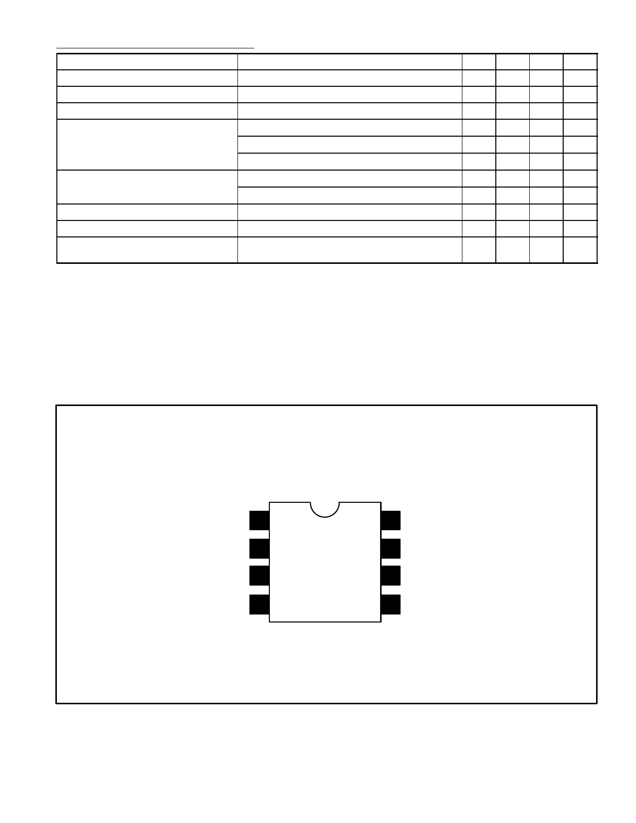
Pin Connection Diagram
Current Limit 1
Booster Output 2
Unregulated Input 3
GND 4
8 Regulated Output
7 Compensation
6 Feedback
5 Reference Bypass
Share Link: 