SG117 데이터 시트보기 (PDF) - Microsemi Corporation
부품명
상세내역
일치하는 목록
SG117 Datasheet PDF : 9 Pages
| |||
SG117 / 217 / 317 / 117A / 217A / 317A
TM
®
1.5A Three Terminal Adj. Voltage Regulator
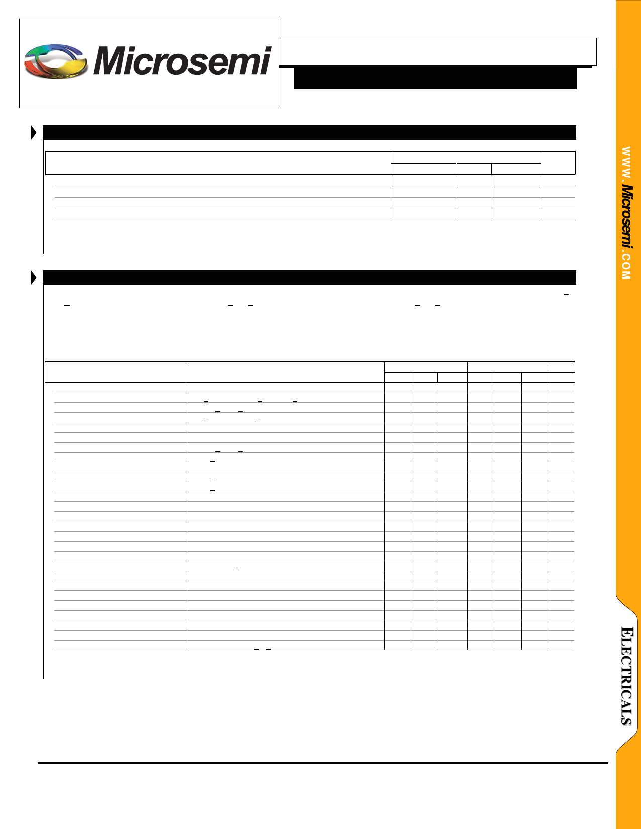
RECOMMENDED OPERATING CONDITIONS
Parameter
Input Voltage Range
Operating Junction Temperature Range
Operating Junction Temperature Range
Operating Junction Temperature Range
SG117A / SG117
SG217A / SG217
SG317A / SG317
SGx17x
Min
Typ
VOUT + 3.5
-55
-25
0
Note 2: Range Over which the device is functional.
Note 3: These ratings are applicable for junction temperatures of less than 150°C
Units
Max
37
V
150
°C
150
°C
125
°C
ELECTRICAL CHARACTERISTICS
Unless otherwise specified, these specifications apply over the full operating ambient temperature for the SG117A / SG117 with -55°C <
TA < 125°C, the SG217A / SG217 with -25°C < TA < 85°C, and the SG317A / SG317 with 0°C < TA < 70°C, VIN – VOUT = 5.0V and for
IOUT = 500mA (K,R, G, and IG) and IOUT = 100mA (T, F, and L packages). Although power dissipation is internally limited, these
specifications are applicable for power dissipations of 2W for the T and L packages, and 20W for the K, R, G, and IG packages. IMAX is
1.5A for the K, R, G, and IG packages and 500m for the T, F, and L packages. Low duty cycle pulse testing techniques are used which
maintains junction and case temperatures equal to the ambient temperature.
Parameter
Reference Voltage
Line Regulation (Note 4)
Load Regulation (Note 4)
Thermal Regulation (Note 5)
Adjust Pin Current
Adjust Pin Current Change
Minimum Load Current
Current Limit
Temperature Stability (Note 5)
Long Term Stability (Note 5)
RMS Output Noise (% of VOUT)
Test Conditions
IOUT = 10mA, TA = 25°C
3V < (VIN – VOUT ) < 40V, P < PMAX
10mA < IOUT < IMAX
3V < (VIN – VOUT) < 40V, IL = 10mA
TA = 25°C
TA = TMIN to TMAX
10mA < IOUT < IMAX
VOUT < 5V, TA = 25°C
VOUT > 5V, TA =25°C
VOUT < 5V
VOUT > 5V
TA = 25°C, 20ms pulse
VOUT = 10V, f = 120Hz
CADJ = 1µF, TA = 25°C
CADJ = 10µF
10mA < IOUT < IMAX, 2.5V < (VIN – VOUT) < 40V
(VIN – VOUT) = 40V
(VIN – VOUT) < 15V
K, P, R, G, IG Packages
T, L Packages
(VIN – VOUT) = 40V, TJ = 25°C
K, P, R, G, IG Packages
T, L Packages
TA = 125°C, 1000 Hours
TA = 25°C, 10Hz < f < 10kHz (Note 5)
SG117A / SG217A SG117 / SG217 Units
Min Typ Max Min Typ Max
1.238 1.250 1.262
V
1.225 1.250 1.270 1.20 1.25 1.30 V
0.005 0.01
0.01 0.02
0.1 0.02 %/V
0.02 0.05 %/V
5 15
0.1 0.3
20 50
0.3 1
0.002 0.02
5 15 mV
0.1 0.3 %
20 50 mV
0.3 1 %
0.03 0.07 %/W
65
65
dB
66 80
66 80
dB
50 100
50 100 µA
0.2 5
0.2 5 µA
3.5 5
3.5 5 mA
1.5 2.2
1.5 2.2
A
0.5 0.8
0.5 0.8
A
0.3 0.4
0.3 0.4
A
0.15 0.2
0.15 0.2
A
1
2
1
%
0.3 1
0.3 1 %
0.001
0.001
%
Copyright © 1994
Rev. 1.3, 2006-02-08
Microsemi
Integrated Products Division
11861 Western Avenue, Garden Grove, CA. 92841, 714-898-8121, Fax: 714-893-2570
Page 3
Share Link: 