BU2090 데이터 시트보기 (PDF) - ROHM Semiconductor
부품명
상세내역
일치하는 목록
BU2090 Datasheet PDF : 12 Pages
| |||
Standard ICs
BU2090 / BU2090F / BU2090FS /
BU2092 / BU2092F / BU2092FV
•Truth table
BU2092 / F / FV
INPUT
CLOCK DATA LCK
×
×
×
×
×
×
L
×
H
×
×
×
×
×
×
×
FUNCTION
OE
H Output (Q0 to Q11) disabled
L Output (Q0 to Q11) enabled
× First cell of the shift register stores the LOW. Other cells, respectively, store
data from the preceding cells or other prior data. (Output state is HOLD.)
×
First cell of the shift register stores the HIGH. Other cells, respectively, store
data from the preceding cells or other prior data. (Storage state and output state are HOLD.)
× No change in shift register.
× Contents of shift register are stored in storage register.
× No change in shift register.
Q0 to Q11 output for the BU2090 / F / FS and BU2092 / F / FV is Nch open drain output. When the shift register transfer data is LOW,
the corresponding output FET is ON (continuous state). When the transfer data is HIGH, the output FET is OFF (discontinuous).
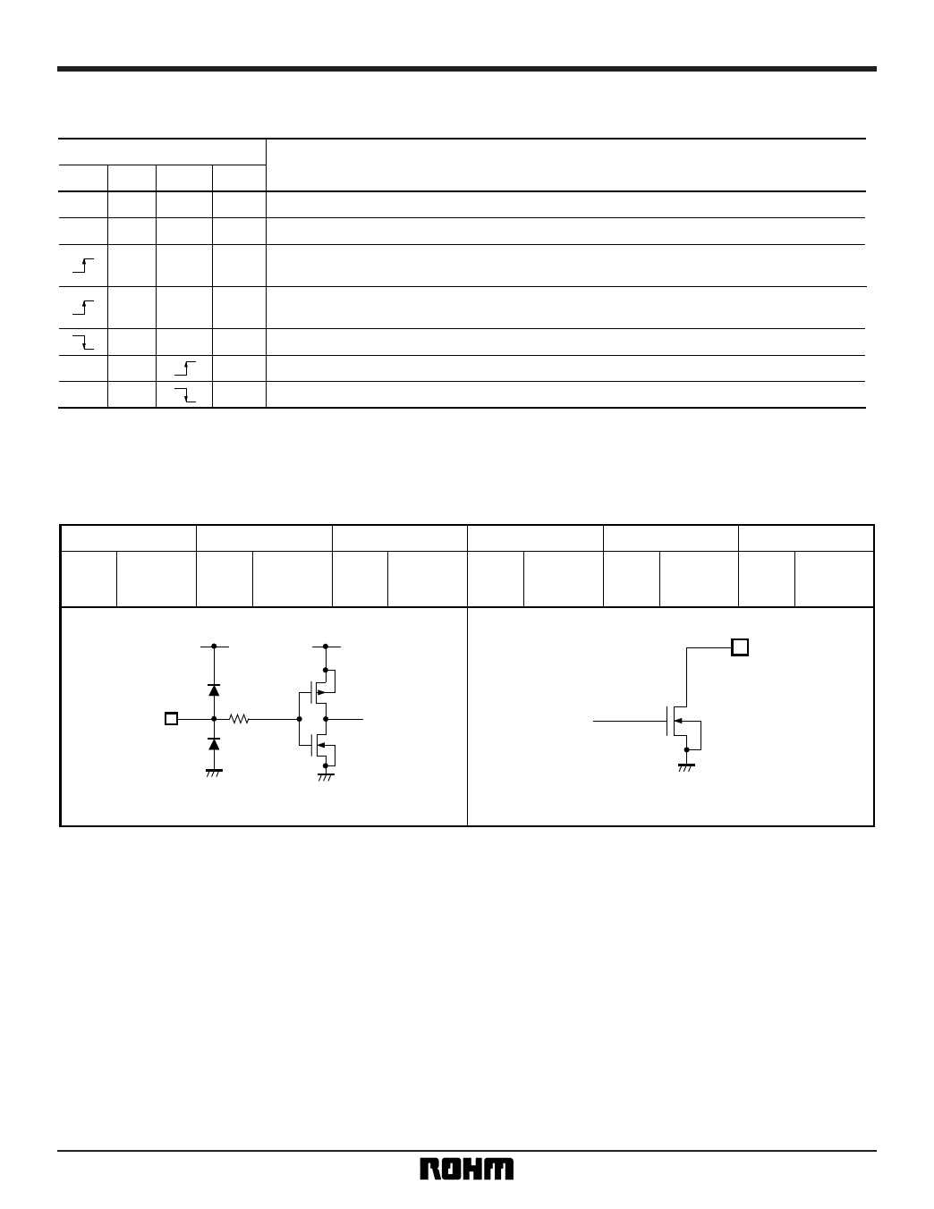
•Input / output circuit
BU2090 / F / FS
BU2092 / F
BU2092FV
BU2090 / F / FS
BU2092 / F
BU2092FV
4, 5, 6, 7, 8, 9
5, 6, 7, 8, 9,
5, 6, 7, 8, 9,
Pin No. 2, 3 Pin No. 2, 3, 4, 17 Pin No. 2, 3, 4, 19 Pin No. 10, 11, 12, 13 Pin No. 10, 11, 12, 13 Pin No. 10, 11, 14, 15
14, 15
14, 15, 16
16, 17, 18
VDD
VDD
GND (VSS)
GND (VSS)
GND (VSS)
7
Share Link: 