TDA3566 데이터 시트보기 (PDF) - Philips Electronics
부품명
상세내역
일치하는 목록
TDA3566 Datasheet PDF : 24 Pages
| |||
Philips Semiconductors
PAL/NTSC decoder
Product specification
TDA3566A
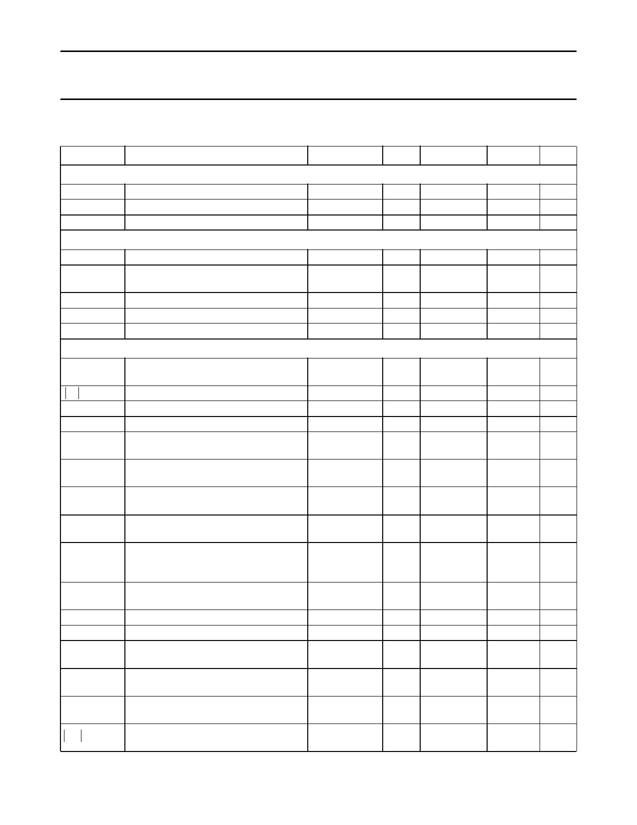
CHARACTERISTICS
VP = 12 V; Tamb = 25 °C; all voltages are referenced to pin 27; unless otherwise specified.
SYMBOL
PARAMETER
CONDITIONS MIN.
TYP.
Supply
VP
supply voltage
IP
supply current
Ptot
total power dissipation
Luminance input (pin 8)
V8(p-p)
V8
input voltage (peak-to-peak value)
input voltage level before clipping
occurs in the input stage
I8
input current
contrast control range
I6
input current contrast control
Chrominance amplifier
V4(p-p)
Z4
C4
∆V
input signal amplitude
(peak-to-peak value)
input impedance
input capacitance
ACC control range
change of the burst signal at the output
control range
G
amplification at nominal saturation
(pin 4 to pin 28)
chrominance to burst ratio at nominal
saturation
V28(p-p)
maximum output voltage range
(peak-to-peak value)
d
distortion of chrominance amplifier at
2 V (p-p) output signal up to an input
signal of 1 V (p-p)
α28-4
frequency response between 0 and
5 MHz
saturation control range
I5
input current saturation control
cross-coupling between luminance and
chrominance amplifier
S/N
signal-to-noise ratio at nominal input
signal
∆ϕ
phase shift burst with respect to
chrominance at nominal saturation
Z28
output impedance of chrominance
amplifier
note 1
see Fig.3
note 2
100 mV to
1 V (p-p)
note 3
RL = 2 kΩ
see Fig.4
note 4
note 5
10.8 12.0
−
90
−
1.1
−
0.45
−
−
−
0.1
−11.5 −
−
−
40
390
−
10
−
−
30
−
−
−
34
−
−
7
4
5
−
−
−
−
50
−
−
−
−
−
56
−
−
−
−
10
MAX. UNIT
13.2
V
120
mA
1.6
W
0.63
V
1.4
V
1
µA
+5
dB
15
µA
1 100
mV
−
kΩ
6.5
pF
−
dB
1
dB
−
dB
−
dB
−
V
5
%
−2
dB
−
dB
20
µA
−46
dB
−
dB
±5
deg
−
Ω
February 1994
8
Share Link: 