74F299SJX 데이터 시트보기 (PDF) - Fairchild Semiconductor
부품명
상세내역
일치하는 목록
74F299SJX
Fairchild Semiconductor

74F299SJX Datasheet PDF : 7 Pages
| |||
Unit Loading/Fan Out
Pin Names
Description
CP
DS0
DS7
S0, S1
MR
OE1, OE2
I/O0–I/O7
Q0, Q7
Clock Pulse Input (Active Rising Edge)
Serial Data Input for Right Shift
Serial Data Input for Left Shift
Mode Select Inputs
Asynchronous Master Reset Input (Active LOW)
3-STATE Output Enable Inputs (Active LOW)
Parallel Data Inputs or
3-STATE Parallel Outputs
Serial Outputs
U.L.
HIGH/LOW
1.0/1.0
1.0/1.0
1.0/1.0
1.0/2.0
1.0/1.0
1.0/1.0
3.5/1.083
150/40(33.3)
50/33.3
Functional Description
The 74F299 contains eight edge-triggered D-type flip-flops
and the interstage logic necessary to perform synchronous
shift left, shift right, parallel load and hold operations. The
type of operation is determined by S0 and S1, as shown in
the Mode Select Table. All flip-flop outputs are brought out
through 3-STATE buffers to separate I/O pins that also
serve as data inputs in the parallel load mode. Q0 and Q7
are also brought out on other pins for expansion in serial
shifting of longer words.
A LOW signal on MR overrides the Select and CP inputs
and resets the flip-flops. All other state changes are initi-
ated by the rising edge of the clock. Inputs can change
when the clock is in either state provided only that the rec-
ommended setup and hold times, relative to the rising edge
of CP, are observed.
A HIGH signal on either OE1 or OE2 disables the 3-STATE
buffers and puts the I/O pins in the high impedance state.
In this condition the shift, hold, load and reset operations
can still occur. The 3-STATE outputs are also disabled by
HIGH signals on both S0 and S1 in preparation for a paral-
lel load operation.
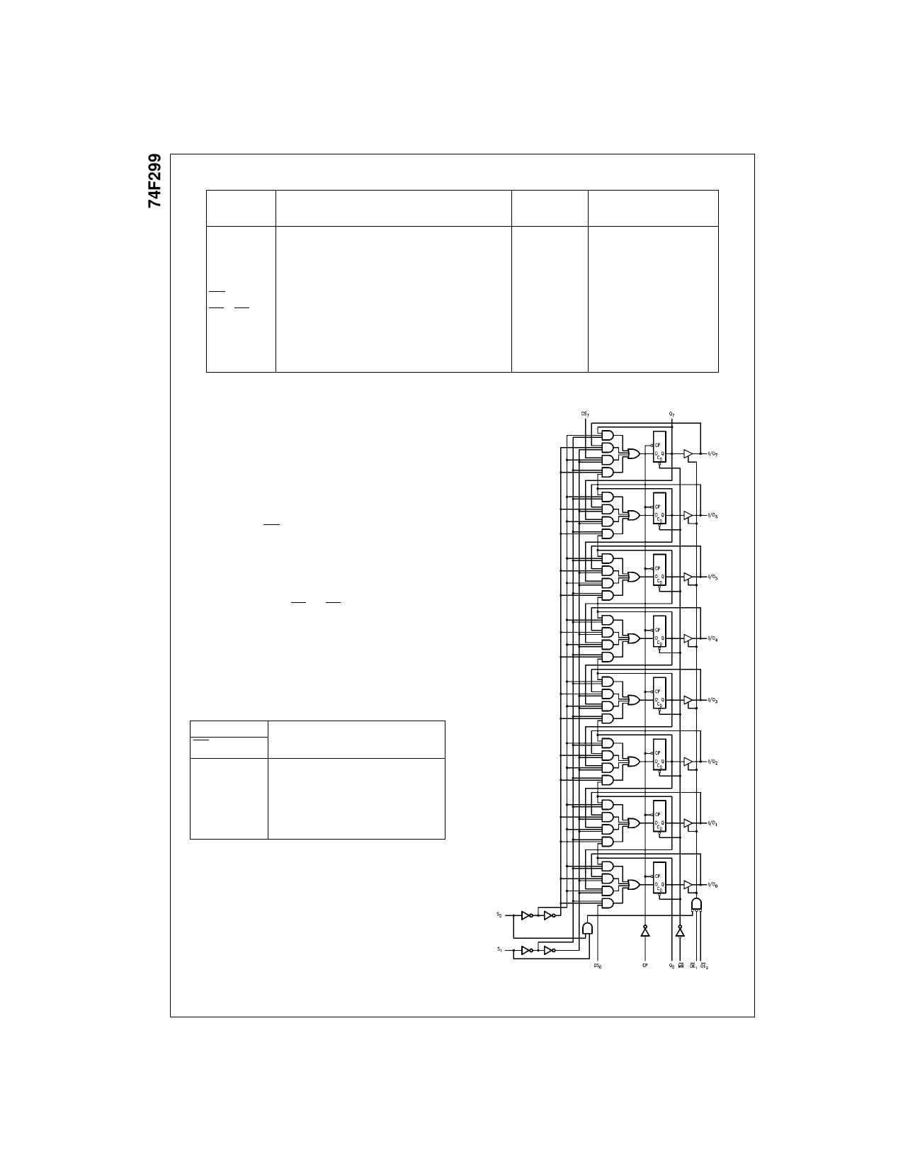
Logic Diagram
Mode Select Table
Inputs
MR S1 S0 CP
Response
L
H
H
H
X
H
L
H
X
H
H
L
X Asynchronous Reset; Q0–Q7 = LOW
Parallel Load; I/On → Qn
Shift Right; DS0 → Q0, Q0 → Q1, etc.
Shift Left; DS7 → Q7, Q7 → Q6, etc.
H L L X Hold
H = HIGH Voltage Level
L = LOW Voltage Level
X = Immaterial
= LOW-to-HIGH Clock Transition
Input IIH/IIL
Output IOH/IOL
20 µA/−0.6 mA
20 µA/−0.6 mA
20 µA/−0.6 mA
20 µA/−1.2 mA
20 µA/−0.6 mA
20 µA/−0.6 mA
70 µA/−0.65 mA
−3 mA/24 mA (20 mA)
−1 mA/20 mA
www.fairchildsemi.com
Please note that this diagram is provided only for the understanding of logic
operations and should not be used to estimate propagation delays.
2
Share Link: