74ABT273CSCX 데이터 시트보기 (PDF) - Fairchild Semiconductor
부품명
상세내역
일치하는 목록
74ABT273CSCX Datasheet PDF : 9 Pages
| |||
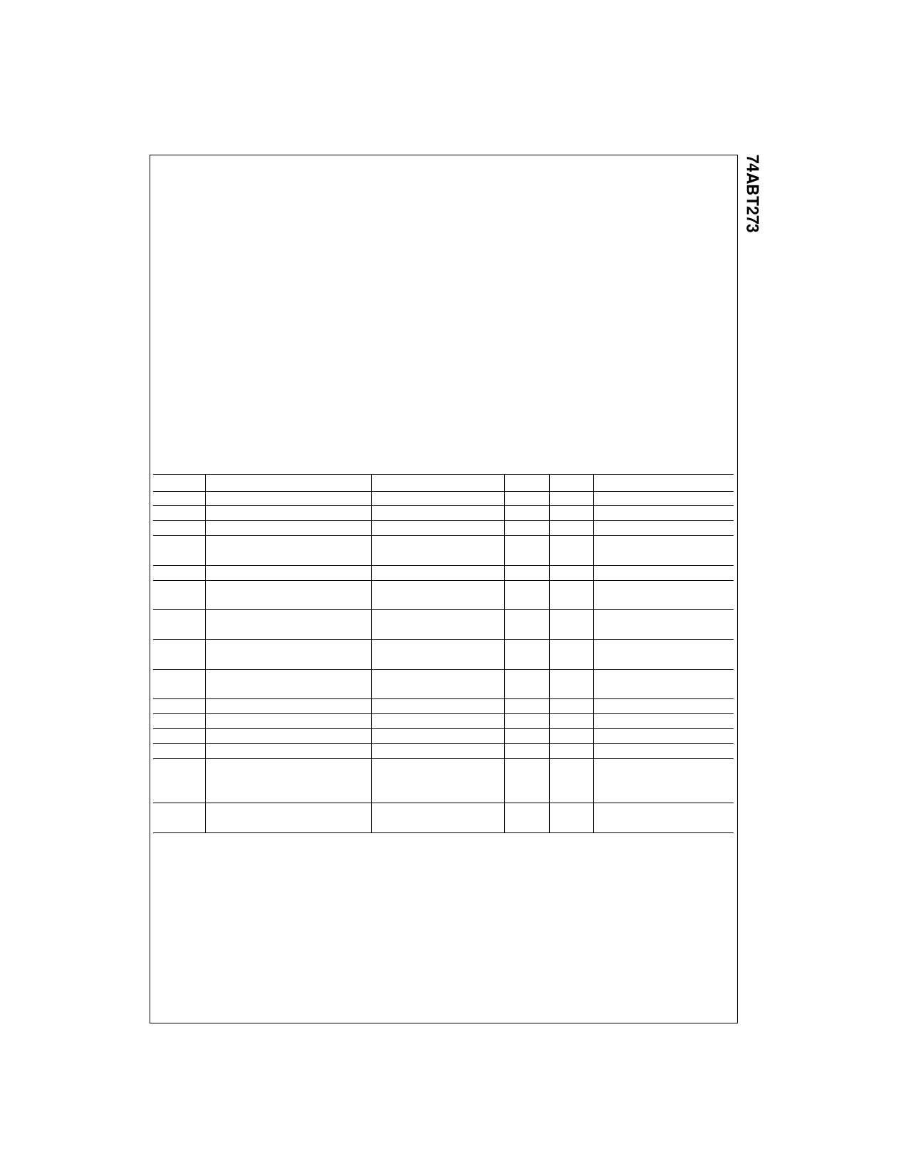
Absolute Maximum Ratings(Note 2)
Storage Temperature
65qC to 150qC
Ambient Temperature under Bias
55qC to 125qC
Junction Temperature under Bias
55qC to 150qC
VCC Pin Potential to Ground Pin
Input Voltage (Note 3)
0.5V to 7.0V
0.5V to 7.0V
Input Current (Note 3)
30 mA to 5.0 mA
Voltage Applied to Any Output
in the Disabled or
Power-Off State
0.5V to 4.75V
in the HIGH State
Current Applied to Output
0.5V to VCC
in LOW State (Max)
DC Latchup Source Current
twice the rated IOL (mA)
500 mA
(Across Comm Operating Range)
Over Voltage Latchup
VCC 4.5V
Recommended Operating
Conditions
Free Air Ambient Temperature
Supply Voltage
Minimum Input Edge Rate ('V/'t)
Data Input
Enable Input
40qC to 85qC
4.5V to 5.5V
50 mV/ns
20 mV/ns
Note 2: Absolute maximum ratings are values beyond which the device
may be damaged or have its useful life impaired. Functional operation
under these conditions is not implied.
Note 3: Either voltage limit or current limit is sufficient to protect inputs.
DC Electrical Characteristics
Symbol
Parameter
Min
Typ
Max
Units
VCC
Conditions
VIH
Input HIGH Voltage
2.0
V
Recognized HIGH Signal
VIL
Input LOW Voltage
0.8
V
Recognized LOW Signal
VCD
Input Clamp Diode Voltage
1.2
V
Min IIN 18 mA
VOH
Output HIGH Voltage
2.5
2.0
V
Min
IOH 3 mA
IOH 32 mA
VOL
Output LOW Voltage
0.55
V
Min IOL 64 mA
IIH
Input HIGH Current
1
PA
Max VIN 2.7V (Note 4)
1
VIN VCC
IBVI
Input HIGH Current
7
PA
Max VIN 7.0V
Breakdown Test
IIL
Input LOW Current
VID
Input Leakage Test
1
PA
Max VIN 0.5V (Note 4)
1
VIN 0.0V
4.75
V
0.0 IID 1.9 PA
All Other Pins Grounded
IOS
ICEX
ICCH
ICCL
ICCT
Output Short-Circuit Current
Output HIGH Leakage Current
Power Supply Current
Power Supply Current
Maximum ICC/Input Outputs Enabled
100
ICCD
Dynamic ICC
No Load
275
50
50
30
1.5
0.3
mA
PA
PA
mA
mA
mA/
MHz
Max
Max
Max
VOUT 0.0V
VOUT VCC
All Outputs HIGH
Max All Outputs LOW
Max VI VCC 2.1V
Data Input VI VCC 2.1V
All Others at VCC or GND
Outputs Open (Note 5)
Max
One Bit Toggling, 50% Duty Cycle
Note 4: Guaranteed but not tested.
Note 5: For 8 bits toggling, ICCD 0.5 mA/MHz.
3
www.fairchildsemi.com
Share Link: 