PI74LCX16652V 데이터 시트보기 (PDF) - Pericom Semiconductor
부품명
상세내역
일치하는 목록
PI74LCX16652V Datasheet PDF : 7 Pages
| |||
PI74LCX16652
12345678901234567890123456789012123456789012345678901234567890121234567890123456789012345678901212314656-7B89i0t1R234e5g67i8s9t0e1r23e4d56T789r0a1n21s2c34e5i6v78e9r0s12
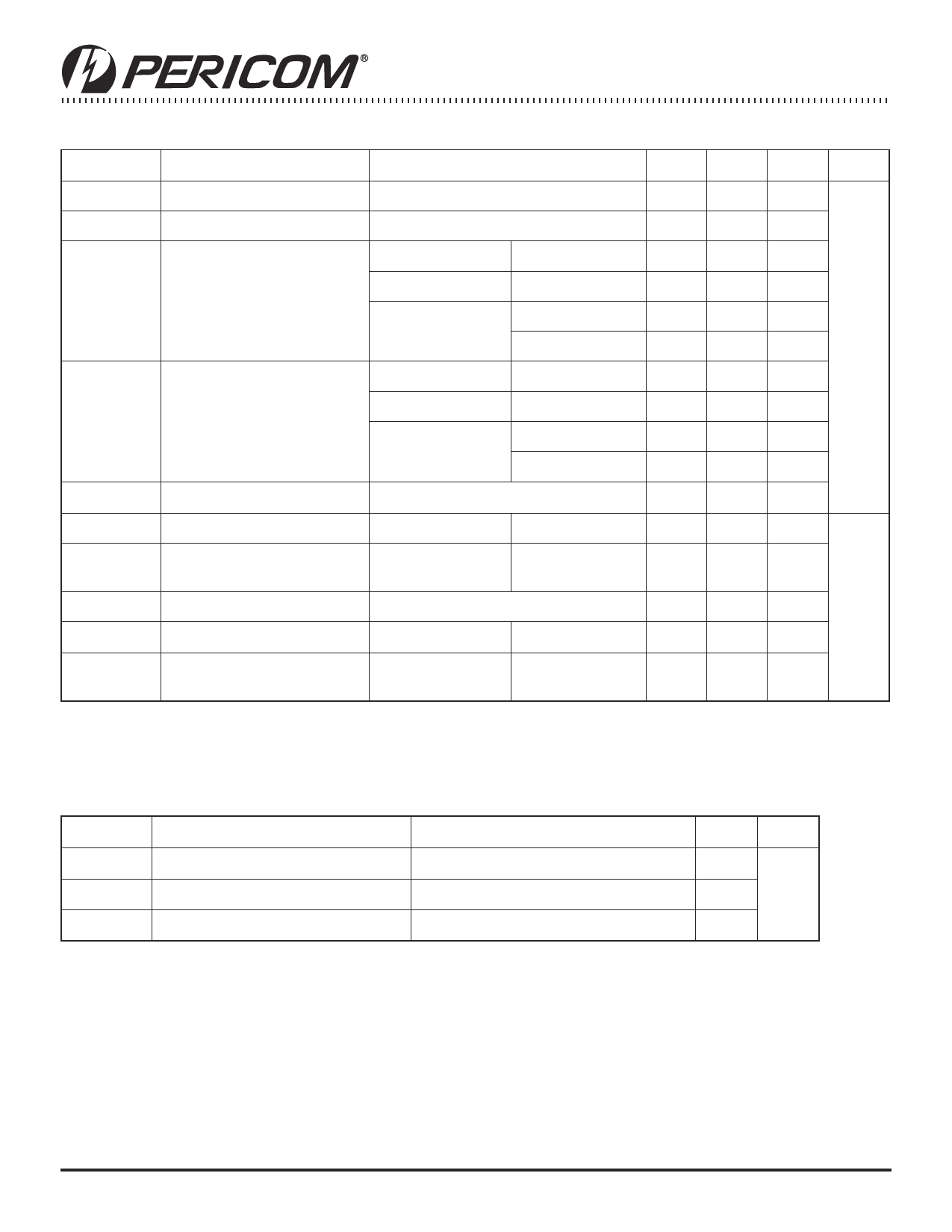
DC Electrical Characteristics (Over the Operating Range, TA = −40°C to +85°C, VCC = 2.7V to 3.6V)
Parameters
VIH
VIL
VOH
VOL
VIK
II
IOZ
IOFF
ICC
∆ICC
Description
Test Conditions(1)
Input HIGH Voltage
Guaranteed Logic HIGH Level
Input LOW Voltage
Guaranteed Logic LOW Level
Output HIGH Voltage
VCC = 2.7-3.6
IOH = –0.1 mA
VCC = 2.7
IOH = –12 mA
VCC = 3.0
IOH = –18 mA
IOH = –24 mA
Output LOW Voltage
VCC = 2.7-3.6
IOL = 0.1 mA
VCC = 2.7
IOL = 12mA
VCC = 3.0
IOL = 16 mA
IOL = 24 mA
Clamp Diode Voltage
VCC = Min., IIN = –18 mA
Input Leakage Current
0 ≤ VI ≤ 5.5V
Vcc = 2.7-3.6
Tri-State Output Leakage
0 ≤ VO ≤ 5.5V
VI = VIH or VIL
VCC = 2.7-3.6
Power Down Disable
VCC = 0V, VIN or VOUT ≤ 5.5V
Quiescent Power Supply Current VCC = Max.
VIN = GND or VCC
Quiescent Power Supply Current VCC = Max.
TTL Inputs HIGH
VIN = VCC – 0.6V(3)
Min.
2.0
—
VCC-0.2
2.2
2.4
2.2
—
—
—
—
—
—
—
—
Typ(2)
—
—
—
—
—
—
—
—
—
—
−0.7
—
—
—
0.1
Max.
—
0.8
—
—
—
—
0.2
0.4
0.4
0.55
−1.2
±5
±5
10
10
500
Units
V
µA
Notes:
1. For Max. or Min. conditions, use appropriate value specified under Electrical Characteristics for the applicable device type.
2. Typical values are at VCC = 3.3V, +25°C ambient.
3. Per TTL driven input; all other inputs at Vcc or GND.
Capacitance
Parameters Description
Test Conditions
Typ. Units
CIN
COUT
CPD
Input Capacitance
Output Capacitance
Power Dissipation Capacitance
VCC = Open, VI = 0V or VCC
7
VCC = 3.3V, VI = 0V or VCC
8
pF
VCC = 3.3V, VI = 0V or VCC, F = 10 MHz
20
5
PS2094B 09/20/02
Share Link: 