XC61CC1302 데이터 시트보기 (PDF) - TOREX SEMICONDUCTOR
부품명
상세내역
일치하는 목록
XC61CC1302 Datasheet PDF : 19 Pages
| |||
XC61C Series
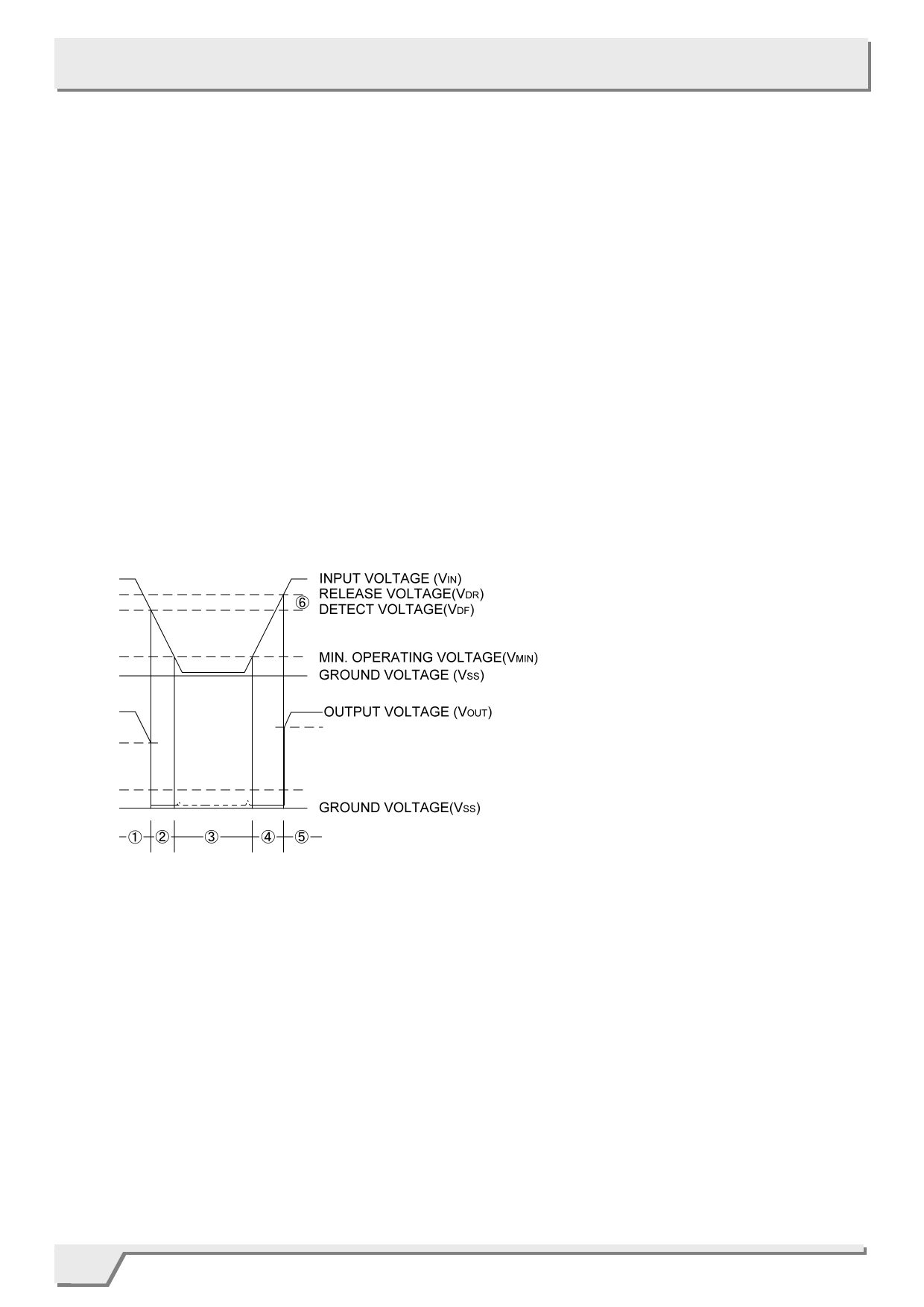
■OPERATIONAL EXPLANATION
(Especially prepared for CMOS output products)
① When input voltage (VIN) rises above detect voltage (VDF), output voltage (VOUT) will be equal to VIN.
(A condition of high impedance exists with N-ch open drain output configurations.)
② When input voltage (VIN) falls below detect voltage (VDF), output voltage (VOUT) will be equal to the ground voltage
(VSS) level.
③ When input voltage (VIN) falls to a level below that of the minimum operating voltage (VMIN), output will become
unstable. In this condition, VIN will equal the pulled-up output (should output be pulled-up.)
④ When input voltage (VIN) rises above the ground voltage (VSS) level, output will be unstable at levels below the
minimum operating voltage (VMIN). Between the VMIN and detect release voltage (VDR) levels, the ground voltage (VSS)
level will be maintained.
⑤ When input voltage (VIN) rises above detect release voltage (VDR), output voltage (VOUT) will be equal to VIN.
(A condition of high impedance exists with N-ch open drain output configurations.)
⑥ The difference between VDR and VDF represents the hysteresis range.
●Timing Chart
10/19
Share Link: 