CS61884 데이터 시트보기 (PDF) - Cirrus Logic
부품명
상세내역
일치하는 목록
CS61884 Datasheet PDF : 71 Pages
| |||
CS61884
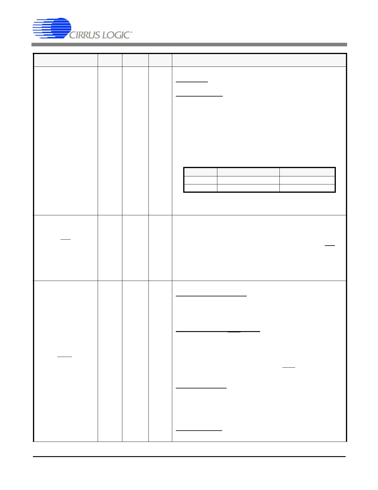
SYMBOL
MUX/BITSEN0
INT
RDY/ACK/SDO
LQFP FBGA TYPE
DESCRIPTION
43
K2
Multiplexed Interface/Bits Clock Select
Host Mode -This pin configures the microprocessor inter-
face for multiplexed or non-multiplexed operation.
Hardware mode - This pin is used to enable channel 0 as
a G.703 BITS Clock recovery channel (Refer to BUILDING
INTEGRATED TIMING SYSTEMS (BITS) CLOCK MODE
I (See Section 8 on page 23). Channel 1 through 7 are not
affected by this pin during hardware mode. During host
mode the G.703 BITS Clock recovery function is enabled by
the Bits Clock Enable Register (1Eh) (See Section 14.31
on page 41).
Table 2. Mux/Bits Clock Selection
Pin State
HIGH
LOW
Parallel Host Mode
multiplexed
non multiplexed
Hardware Mode
BITS Clock ON
BITS Clock OFF
NOTE: The MUX pin only controls the BITS Clock function in
Hardware Mode
Interrupt Output
This active low output signals the host processor when one
of the CS61884’s internal status register bits has changed
82
K13
O state. When the status register is read, the interrupt is
cleared. The various status changes that would force INT
active are maskable via internal interrupt enable registers.
NOTE: This pin is an open drain output and requires a 10 kΩ
pull-up resistor.
Data Transfer Acknowledge/Ready/Serial Data Output
Intel Parallel Host Mode - During a read or write register
access, RDY is asserted “Low” to acknowledge that the de-
vice has been accessed. An asserted “High” acknowledges
that data has been written or read. Upon completion of the
bus cycle, this pin High-Z.
Motorola Parallel Host Mode - During a data bus read
operation this pin “ACK” is asserted “High” to indicate that
data on the bus is valid. An asserted “Low” on this pin dur-
ing a write operation acknowledges that a data transfer to
83
K14
O
the addressed register has been accepted. Upon comple-
tion of the bus cycle, this pin High-Z.
NOTE: Wait state generation via RDY/ACK is disabled in
RZ mode (No Clock Recovery).
Serial Host Mode - When the microprocessor interface is
configured for serial bus operation, “SDO” is used as a seri-
al data output. This pin is forced into a high impedance
state during a serial write access. The CLKE pin controls
whether SDO is valid on the rising or falling edge of SCLK.
Upon completion of the bus cycle, this pin High-Z.
Hardware Mode - This pin is not used and should be left
open.
DS485F1
11
Share Link: 