W83194R-17 데이터 시트보기 (PDF) - Winbond
부품명
상세내역
일치하는 목록
W83194R-17 Datasheet PDF : 21 Pages
| |||
W83194R-17/-17A
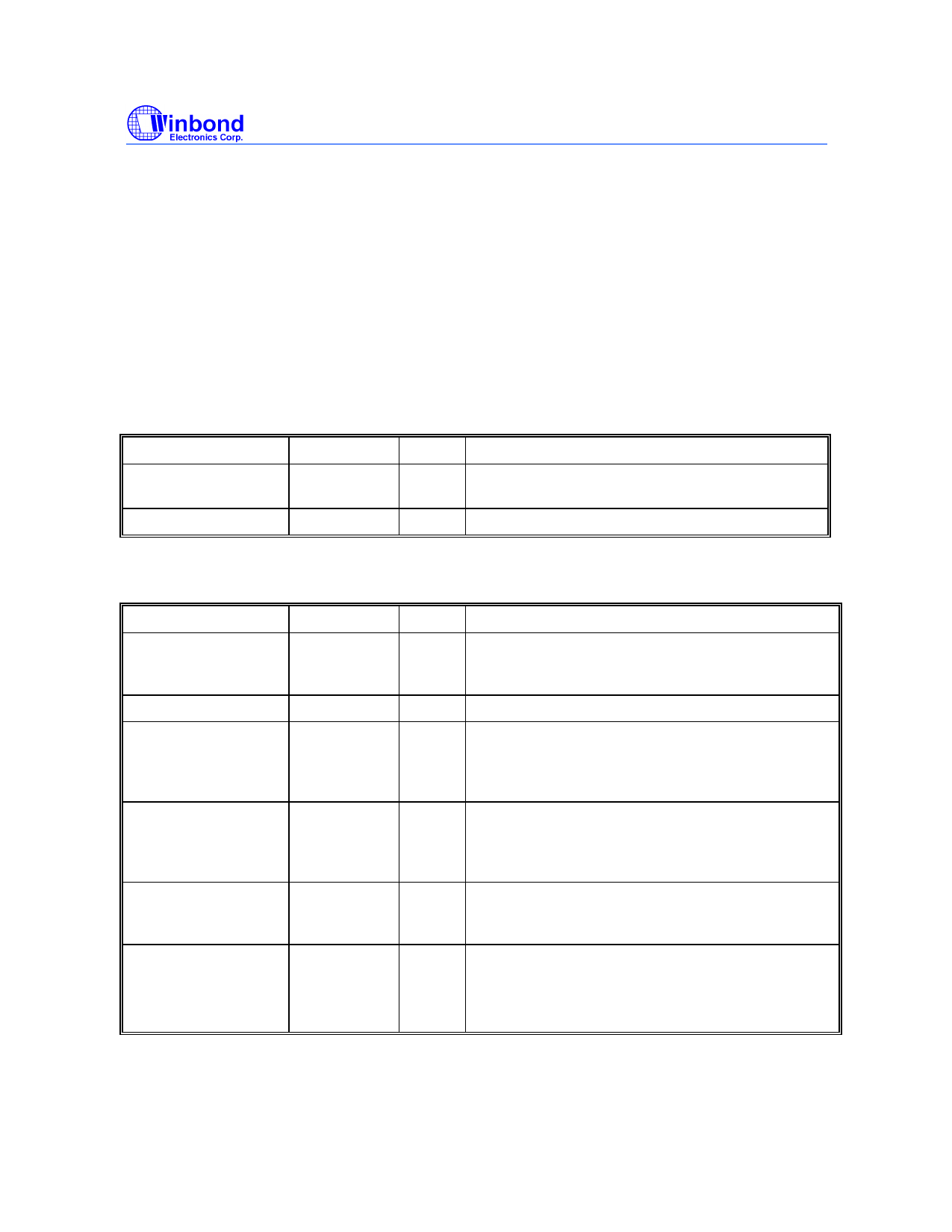
5.0 PIN DESCRIPTION
IN - Input
OUT - Output
I/O - Bi-directional Pin
# - Active Low
* - Internal 250kΩ pull-up
PRELIMINARY
5.1 Crystal I/O
SYMBOL
Xin
Xout
PIN
I/O
FUNCTION
4
IN Crystal input with internal loading capacitors and
feedback resistors.
5
OUT Crystal output at 14.318MHz nominally.
5.2 CPU, SDRAM, PCI Clock Outputs
SYMBOL
CPUCLK [ 0:3 ]
AGP[ 0:1]
SDRAM11/
CPU_STOP#
SDRAM10/
PCI_STOP#
SDRAM [ 0:9]
PCICLK_F/ *FS1
PIN
40,41,43,44
15,47
17
18
20,21,28,29,31
,32,34,
35,37,38
7
I/O
OUT
OUT
I/O
I/O
O
I/O
FUNCTION
Low skew (< 250ps) clock outputs for host
frequencies such as CPU, Chipset and Cache.
Vddq2b is the supply voltage for these outputs.
Accelerate Graphic Port clock outputs
If MODE =1 (default), then this pin is a SDRAM
Clock buffered output. If MODE = 0 , then this pin is
CPU_STOP# input used in power management
mode for synchronously stopping the all CPU clocks.
If MODE = 1 (default), then this pin is a SDRAM
clock output. If MODE = 0 , then this pin is
PCI_STOP # and used in power management mode
for synchronously stopping the all PCI clocks.
SDRAM clock outputs which have the same
frequency as CPU clocks.
Latched input for FS1 at initial power up for H/W
selecting the output frequency of CPU, SDRAM and
PCI clocks.
Free running PCI clock during normal operation.
Publication Release Date: Sep. 1998
-3-
Revision 0.20
Share Link: 