TDA9861 데이터 시트보기 (PDF) - Philips Electronics
부품명
상세내역
일치하는 목록
TDA9861 Datasheet PDF : 18 Pages
| |||
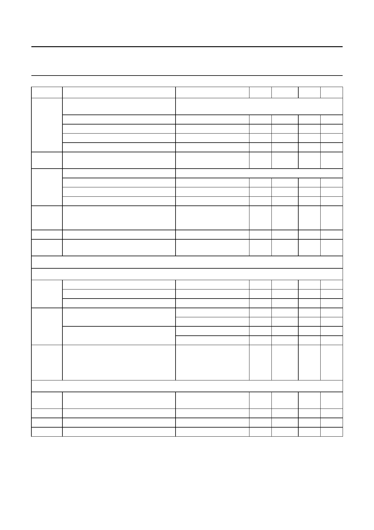
Philips Semiconductors
Universal HiFi audio processor for TV
Preliminary specification
TDA9861
SYMBOL
PARAMETER
VN(W)
weighted noise voltage at output
(quasi-peak level)
for +15 dB gain
for 0 dB gain
for −40 dB gain
for mute position
B
AF bandwidth
CONDITIONS
CCIR468-3
Gv = −80 dB
−1 dB
THD
αsp
total harmonic distortion
for Vi = 0.2 V (RMS value)
for Vi = 1 V (RMS value)
for Vi = 2 V (RMS value)
stereo channel separation
αbus
RR100
crosstalk of I2C-bus
ripple rejection with 100 Hz ripple on
VP
f = 20 to 12500 Hz
Gv = −30 to + 15 dB
Gv = −30 to 0 dB
Gv = −30 to −6 dB
f = 10 kHz; Gv = 0 dB;
opposite input grounded
by 1 kΩ resistor
Gv = 0 dB; note 1
Gv = 0 dB;
VR < 200 mV RMS
HEADPHONE CHANNEL (controlled via I2C-bus, Table 3)
Volume control headphone channel
f = 1 kHz, 36 steps
Gv
nominal volume control
minimum volume control
gain in mute position
∆Gv
step width (resolution)
gain set error
∆V13, 20 DC offset voltage
Gv = −36 to +16 dB
Gv = −54 to −36 dB
Gv = −36 to +16 dB
Gv = −54 to +36 dB
for adjoining step and
any step to mute
Gv = 0 to +16 dB/mute
Gv = −54 to 0 dB/mute
Headphone channel output (pins 13 and 20)
Vo
maximum output signal (RMS value)
THD ≤ 0.5%; RL > 10 kΩ;
CL < 1.5 nF
Ro
output resistance
RL
allowed output load resistor
CL
allowed output load capacitor
MIN.
−
−
−
−
−
−
−
−
−
−
−
−54
−51
−80
1.5
1
−
−
−
−
2
−
10
−
TYP.
102
32
27
20
20 to
20000
0.1
0.1
0.1
75
100
55
−
−
−85
2
2
−
−
2
0.5
−
−
−
−
MAX. UNIT
−
µV
−
µV
−
µV
−
µV
−
Hz
0.3 %
0.3 %
0.3 %
−
dB
−
dB
−
dB
+16 dB
−1
dB
−
dB
2.5 dB
3
dB
1
dB
3
dB
15
mV
10
mV
−
V
100 Ω
−
kΩ
1.5 nF
June 1994
8
Share Link: 