P4C168-35PM 데이터 시트보기 (PDF) - Semiconductor Corporation
부품명
상세내역
일치하는 목록
P4C168-35PM Datasheet PDF : 15 Pages
| |||
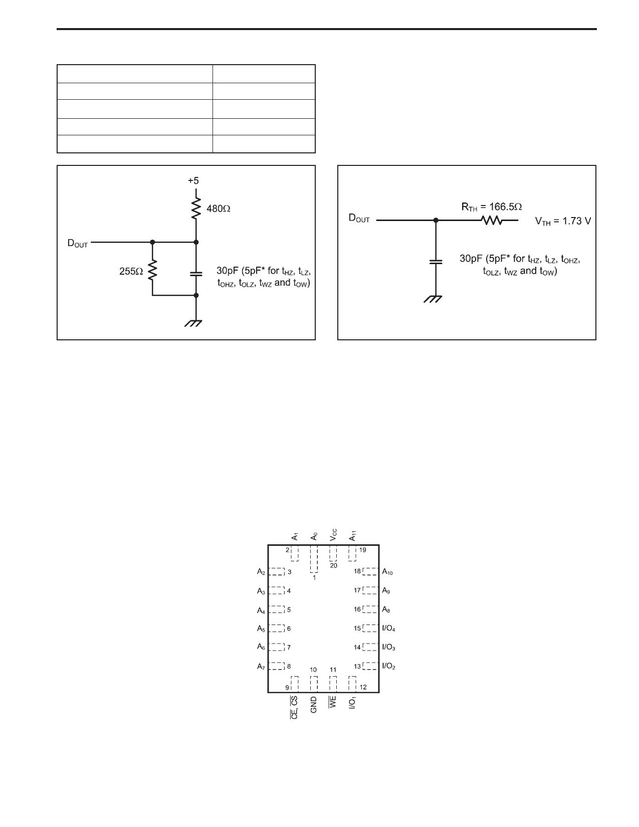
AC TEST CONDITIONS
Input Pulse Levels
Input Rise and Fall Times
Input Timing Reference Level
Output Timing Reference Level
Output Load
GND to 3.0V
3ns
1.5V
1.5V
See Figures 1 and 2
P4C168, P4C169, P4C170
Figure 1. Output Load
* including scope and test fixture.
Note:
Because of the ultra-high speed of the P4C168, P4C169 AND P4C170
care must be taken when testing these devices; an inadequate setup
can cause a normal functioning part to be rejected as faulty. Long high-
inductance leads that cause supply bounce must be avoided by bringing
the VCC and ground planes directly up to the contactor fingers. A high
frequency capacitor of 0.01 µF is also required between VCC and ground.
Figure 2. Thevenin Equivalent
To avoid signal reflections, proper termination must be used; for
example, a 50Ω test environment should be terminated into a 50Ω load
with 1.73V (Thevenin Voltage) at the comparator input, and a 116Ω
resistor must be used in series with DOUT to match 166Ω (Thevenin
Resistance).
LCC PIN CONFIGURATION
Document # SRAM107 REV A
LCC (L9)
Page 7 of 15
Share Link: 