P4C165 데이터 시트보기 (PDF) - Semiconductor Corporation
부품명
상세내역
일치하는 목록
P4C165 Datasheet PDF : 9 Pages
| |||
P4C165
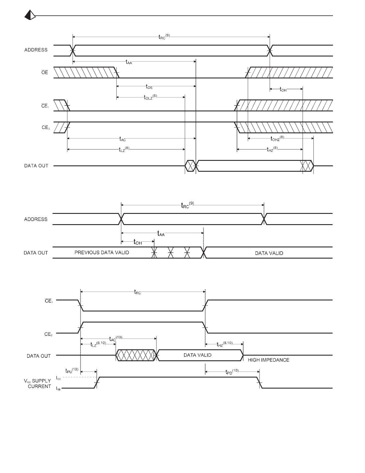
READ CYCLE NO. 1 (OE CONTROLLED)(5)
READ CYCLE NO. 2 (ADDRESS CONTROLLED)(5,6)
READ CYCLE NO. 3 (CE1, CE2 CONTROLLED)(5,7,10)
Notes:
5. WE is HIGH for READ cycle.
6. CE1 is LOW, CE2 is HIGH and OE is LOW for READ cycle.
7. ADDRESS must be valid prior to, or coincident with CE1 transition
LOW and CE2 transition HIGH.
8. Transition is measured ± 200 mV from steady state voltage prior to
change, with loading as specified in Figure 1. This parameter is
sampled and not 100% tested.
9. READ Cycle Time is measured from the last valid address to the first
transitioning address.
10. Transitions caused by a chip enable control have similar delays
irrespective of whether CE1 or CE2 causes them.
Document # SRAM117 Rev OR
4
Page 4 of 9
Share Link: 