BS616LV2013 데이터 시트보기 (PDF) - Brilliance Semiconductor
부품명
상세내역
일치하는 목록
BS616LV2013 Datasheet PDF : 11 Pages
| |||
BSI
BS616LV2013
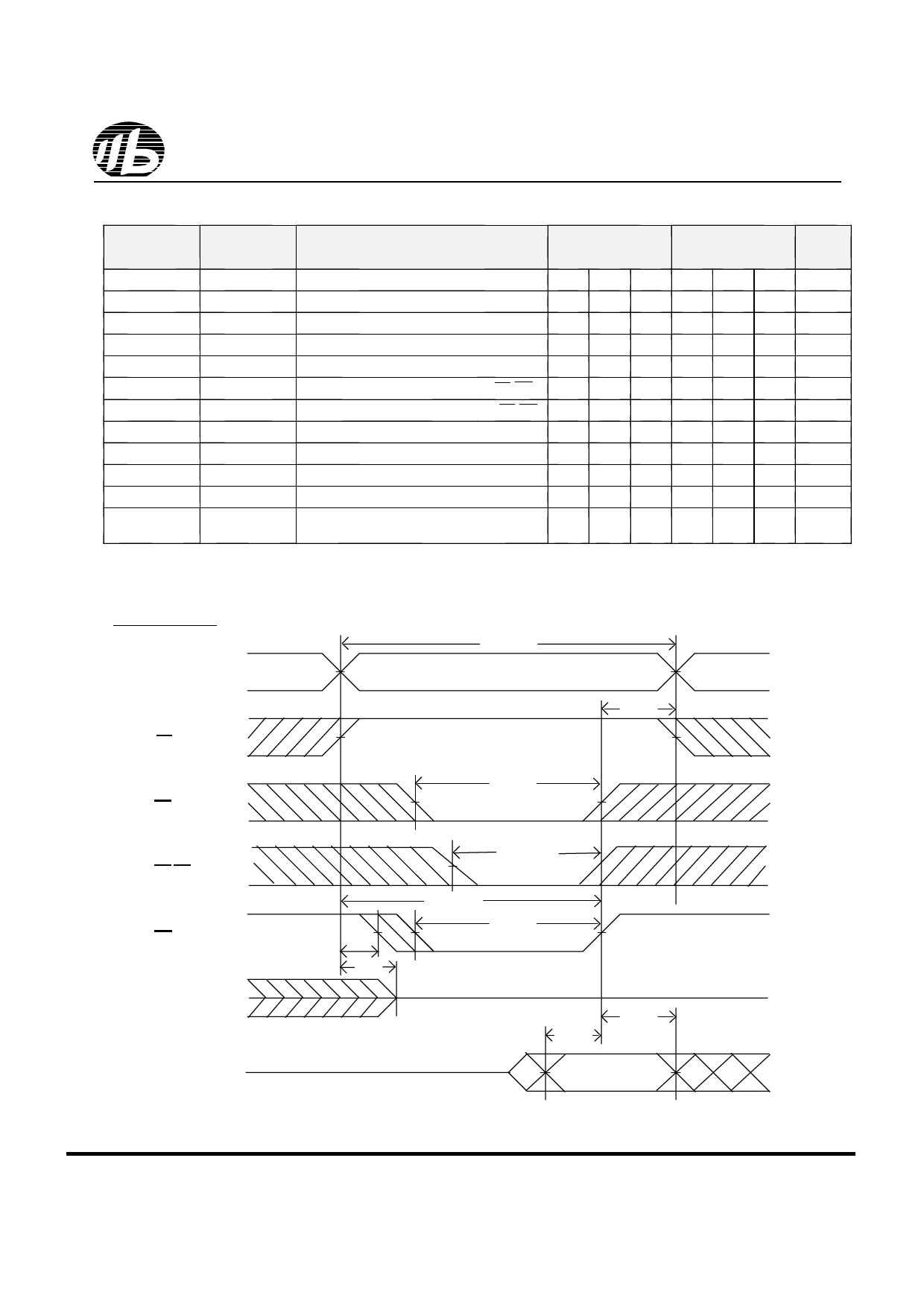
AC ELECTRICAL CHARACTERISTICS ( TA = 0 to + 70oC , Vcc = 3.0V )
WRITE CYCLE
JEDEC
PARAMETER
NAME
t
AVAX
tE1LWH
t
AVWL
tAVWH
t
WLWH
t
WHAX
tBW
t
WLQZ
t
DVWH
t
WHDX
tGHQZ
t
WHOX
PARAMETER
NAME
tWC
tCW
tAS
tAW
tWP
tWR
t (1)
BW
tWHZ
tDW
tDH
tOHZ
tOW
DESCRIPTION
Write Cycle Time
Chip Select to End of Write
Address Setup Time
Address Valid to End of Write
Write Pulse Width
Write recovery Time
Date Byte Control to End of Write
Write to Output in High Z
Data to Write Time Overlap
Data Hold from Write Time
Output Disable to Output in High Z
End of Write to Output Active
(CE,WE)
(LB,UB)
BS616LV2013-70
MIN. TYP. MAX.
70 --
--
70 --
--
0
--
--
70 --
--
35 --
--
0
--
--
30 --
--
0
-- 30
30 --
--
0
--
--
0
-- 30
5
--
--
BS616LV2013-10
MIN. TYP. MAX.
100 --
--
100 --
--
0
--
--
100 --
--
50 --
--
0
--
--
40 --
--
0
-- 40
40 --
--
0
--
--
0
-- 40
10 --
--
UNIT
ns
ns
ns
ns
ns
ns
ns
ns
ns
ns
ns
ns
NOTE :
1. tBW is 30ns/40ns (@speed=70ns/100ns) with address toggle. ; tBW is 70ns/100ns (@speed=70ns/100ns) without address toggle.
SWITCHING WAVEFORMS (WRITE CYCLE)
WRITE CYCLE1 (1)
t WC
ADDRESS
OE
CE
(11)
t CW
(5)
(3)
t WR
LB,UB
WE
D OUT
t AS
(4,10)
t OHZ
t BW
t AW
(3)
t WP
(2)
t DW
t DH
D IN
R0201-BS616LV2013
6
Revision 2.5
April 2002
Share Link: 