NJU3503M 데이터 시트보기 (PDF) - Japan Radio Corporation
부품명
상세내역
일치하는 목록
NJU3503M Datasheet PDF : 60 Pages
| |||
NJU3503
• PORTD(PD0 − PD3)
PORTD is a 4-bit input-output PORT. It operates also as the multiplexed 4-bit analog signal input
terminals (AIN0 to AIN3) to the internal A/D converter by the mask option. The input or the output is
selected for each bit by the mask option. When the PORT is set as the output, the 4-bit signals are output
through the output terminals by writing data into the peripheral register assigned for PORTD (PHY20).
PHY20 as the output register should be written the output data, because the conditions of the output
terminals are unknown while the output data is not written in PHY20. When this PORT is set as the input,
the 4-bit external signals are gotten directly through the input terminals by reading data from PHY20.
Though the output circuit is Nch open drain type, the C-MOS input buffer is connected to the same
terminal. Therefore, the operating current of the chip by the short circuit current when the middle level
voltage between VDD and VSS is input to this terminal.
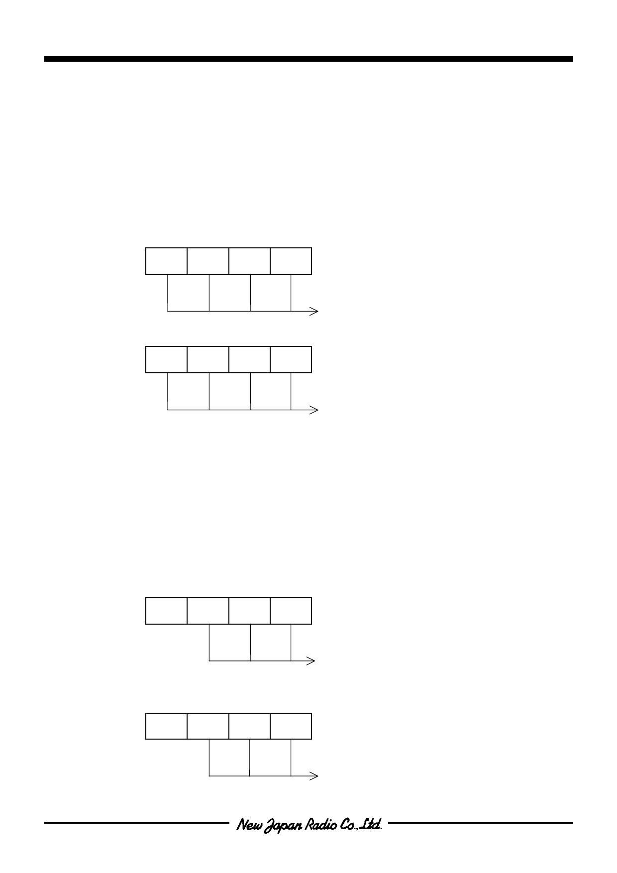
[ READING PORTD INPUT DATA (PHY20) ]
(MSB) 3
2
1
0 (LSB)
PHY20 PD3 PD2 PD1 PD0
PORTD Input Data
[ WRITING PORTD OUTPUT DATA (PHY20) ]
(MSB) 3
2
1
0 (LSB)
PHY20 PD3 PD2 PD1 PD0
PORTD Output Data
• PORTE(PE0 − PE2)
PORTE is a 3-bit input-output PORT. It operates also as the multiplexed 2-channel analog signal input
terminals (AIN4 to AIN5) to the internal A/D converter by the mask option. The input or the output is
selected for each bit by the mask option. When the PORT is set as the output, the 3-bit signals are
output through the output terminals by writing data into the peripheral register assigned for PORTD
(PHY21). PHY21 as the output register should be written the output data, because the conditions of the
output terminals are unknown while the output data is not written in PHY21. When this PORT is set as
the input, the 3-bit external signals are gotten directly through the input terminals by reading data from
PHY21.
Though the output circuit is Nch open drain type, the C-MOS input buffer is connected to the same
terminal. Therefore, the operating current of the chip by the short circuit current when the middle level
voltage between VDD and VSS is input to this terminal.
[ READING PORTE INPUT DATA (PHY21) ]
(MSB) 3
2
1
0 (LSB)
PHY21 “0”
PE2 PE1 PE0
PORTE Input Data
[ WRITING PORTE OUTPUT DATA (PHY21) ]
(MSB) 3
2
1
0 (LSB)
PHY21 −
PE2 PE1 PE0
PORTE Output Data
- 16 -
Share Link: 