NCV8843DG(2010) 데이터 시트보기 (PDF) - ON Semiconductor
부품명
상세내역
일치하는 목록
NCV8843DG Datasheet PDF : 16 Pages
| |||
NCV8843
ELECTRICAL CHARACTERISTICS (continued) (−40°C < TJ < 150°C, 4.5 V< VIN < 40 V; unless otherwise specified.)
Characteristic
Test Conditions
Min
Typ
Max
General
Quiescent Current
Shutdown Quiescent Current
Boost Operating Current
Minimum Boost Voltage
ISW = 0 A
VSHDNB = 0 V, −40°C < TJ < 125°C
VBOOST − VSW = 2.5 V
(Note 6)
−
4.0
7.5
−
1.0
5.0
6.0
15
40
−
−
2.5
Startup Voltage
−
3.0
3.5
4.0
Minimum Output Current
−
6. Guaranteed by design, not 100% tested in production.
−
7.0
12
Unit
mA
mA
mA/A
V
V
mA
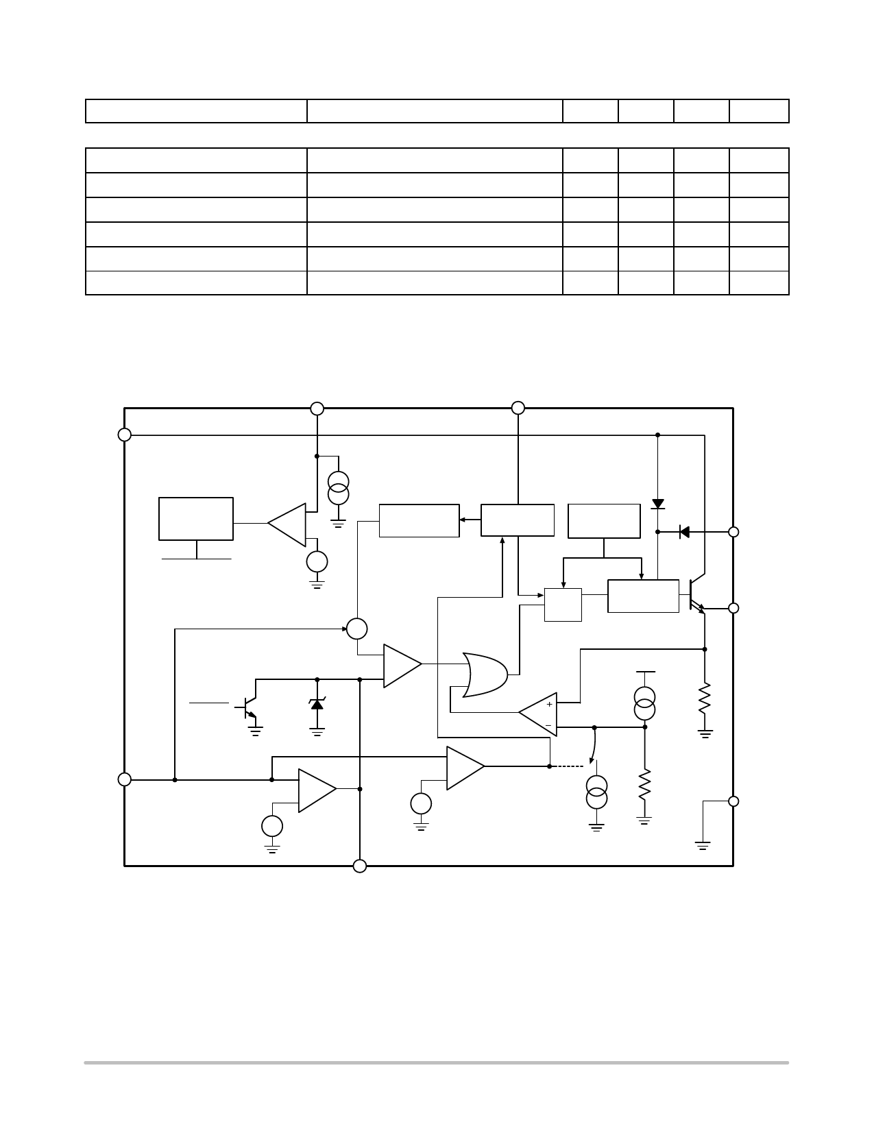
SHDNB
SYNC
VIN
2.9 V LDO
Voltage
Regulator
Internal rail
Shutdown
Comparator
+
−
1.2 V
+
−
4 mA
Artificial
Ramp
SHDNB
1.46 V
∑
+
−
PWM Com-
parator
Oscillator
Thermal
Shutdown
SQ
R
Output
Driver
Current
Limit Com-
parator
IREF
−
VFB
−
+
+
0.32 V
+
−
Frequency IFOLDBACK
and Current
1.27 V
+
−
Error
Amplifier
Limit Foldback
VC
Figure 2. Block Diagram
BOOST
VSW
GND
http://onsemi.com
5
Share Link: 