ML7012-04 데이터 시트보기 (PDF) - Oki Electric Industry
부품명
상세내역
일치하는 목록
ML7012-04 Datasheet PDF : 22 Pages
| |||
1Semiconductor
FEDL 7012-04-01
ML7012-04
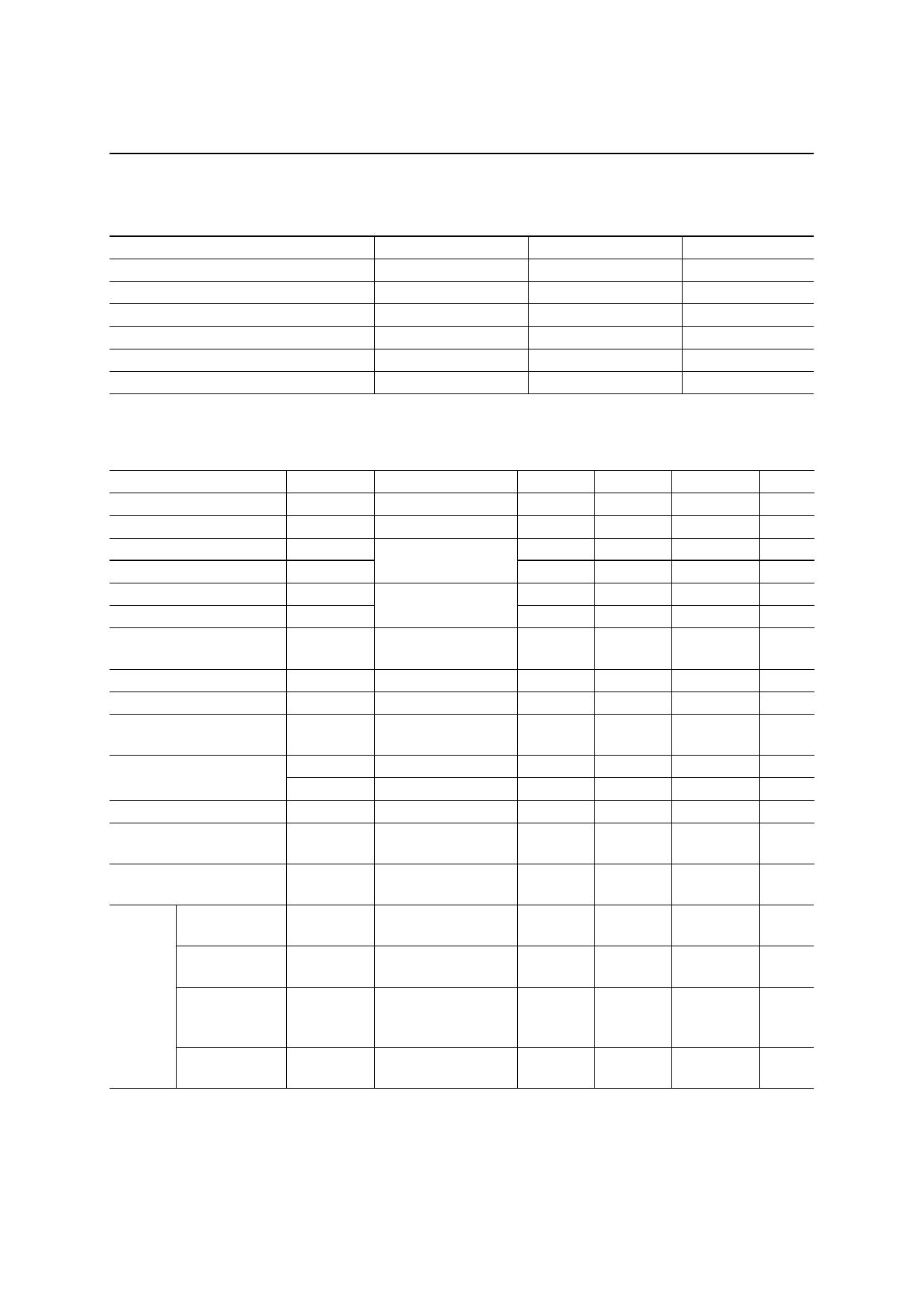
Absolute Maximum Ratings
Parameter
Power Supply Voltage
Analog Input Voltage
Digital Input Voltage
Power dissipation
Output short-circuit current
Storage Temperature
Symbol
Rating
Unit
VDD
VAIN
VDIN
PD
VOUT
TSTG
–0.3 to +5.0
V
–0.3 to VDD +0.3
V
–0.3 to VDD +0.3
V
to 500
mW
to 90
mA
–55 to +150
°C
Recommended Operating Conditions
Parameter
Power Supply Voltage
Operating Temperature
High Level Input Voltage
Low Level Input Voltage
Digital Input Rise time
Digital Input Fall Time
Input Clock Frequency
Deviation
Master CLK Duty
Digital Output Load
R1 to R3 Resistance Ratio
(R3/R1)
R4 to R5 Resistance Ratio
(R5/R4)
SG Bypass Capacitor
Oscillator Feedback
Resistance
OSC0 and OSC1 Load
Capacitance
Oscillation
Frequency
Crystal
Frequency
Deviation
Equivalent
Series
Resistance *1
Load
Capacitance *1
Symbol
VDD
TOP
VIH
VIL
tir
tif
FMCK
DMCK
CDL
Rrat1
Rrat2
Rrat3
CSG
ROSC
C01, C02
Condition
—
—
All digital input pins
excluding OSC0
All digital input pins
Min.
2.7
–20
0.7 × VDD
0
—
—
11.0592 MHz
–100
Input to OSC0
40
Digital output pin
—
—
—
VDD ≥ 3 V
—
VDD ≥ 2.7 V
—
SG pin
1
Between OSC0 and
800
OSC1
OSC0 and OSC1 pins —
Typ.
—
+25
—
—
—
—
—
50
—
1
—
—
—
1000
15
Max.
3.6
+70
VDD
0.16 × VDD
20
20
+100
60
50
1.05
2
1.6
—
1200
Unit
V
°C
V
V
ns
ns
ppm
%
pF
—
—
—
µF
kΩ
—
pF
—
—
—
11.0592
—
MHz
—
Including temperature
characteristics
–80
—
+80
ppm
—
—
—
—
90
Ω
—
—
—
12
—
pF
*1: If the crystal manufacturer’s evaluation is sufficiently verified, the values of equivalent series resistance and
load capacitance may be changeable so long as the frequency deviation is within the range specified above.
7/22
Share Link: 