EDS1232AATA-75MI 데이터 시트보기 (PDF) - Elpida Memory, Inc
부품명
상세내역
일치하는 목록
EDS1232AATA-75MI Datasheet PDF : 53 Pages
| |||
EDS1232AATA-MI
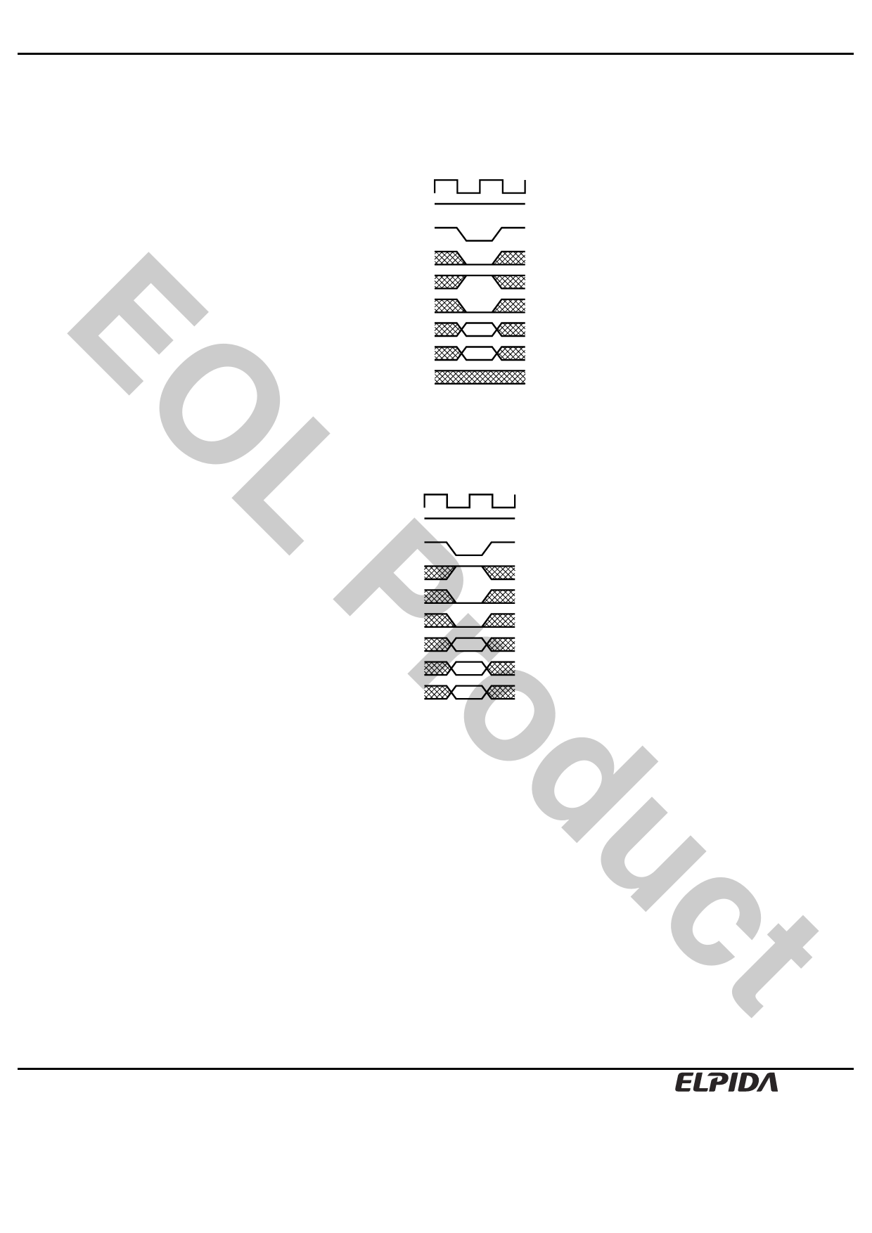
Precharge command (/CS, /RAS, /WE = Low, /CAS = High)
This command begins precharge operation of the bank selected by BA0 and BA1. When A10 is High, all banks are
precharged, regardless of BA0 and BA1. When A10 is Low, only the bank selected by BA0 and BA1 is precharged.
After this command, the Synchronous DRAM can’t accept the activate command to the precharging bank during tRP
(precharge to activate command period). This command corresponds to a conventional DRAM’s /RAS rising.
CLK
CKE H
/CS
/RAS
/CAS
/WE
E BA0, BA1
(Bank select)
A10
(Precharge select)
Add
O Precharge Command
Write command (/CS, /CAS, /WE = Low, /RAS = High)
If the mode register is in the burst write mode, this command sets the burst start address given by the column
address to begin the burst write operation. The first write data in burst mode can input with this command with
subsequent data on following clocks.
L CLK
CKE H
/CS
/RAS
P/CAS
/WE
BA0, BA1
(Bank select)
rA10
Add
Col.
oduct Column Address and Write Command
Data Sheet E0340E30 (Ver. 3.0)
12
Share Link: 