PDM31564 데이터 시트보기 (PDF) - Paradigm Technology
부품명
상세내역
일치하는 목록
PDM31564 Datasheet PDF : 9 Pages
| |||
PRELIMINARY
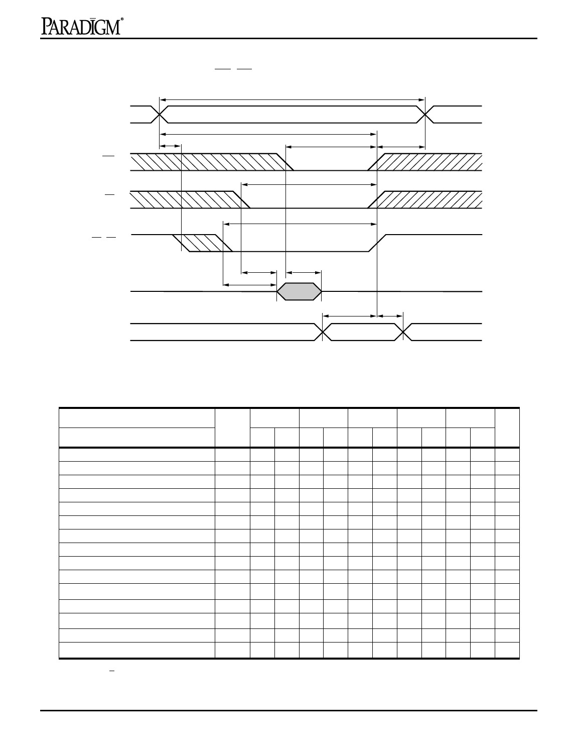
Write Cycle 3 Timing Diagram (UB, LB Controlled)
ADDRESSES
tAS
WE
tWC
tAW
tWP
tAH
tCW
CE
tBW
UB, LB
DOUT
DIN
tLZCE(1)
tLZBE(1)
tHZWE(1)
High Impedance
tDS
tDH
Data Stable
PDM31564
AC Electrical Characteristics
Description
-8*
-10*
-12
-15
-20
WRITE Cycle
WRITE cycle time
Chip enable to end of write
Address valid to end of write
Byte pulse width
Address setup time
Address hold from end of write
Write pulse width
Data setup time
Data hold time
Byte disable to output in low Z(1, 3, 4)
Byte enable to output in high Z(1, 3, 4)
Output disable to output in low Z(1, 3, 4)
Output enable to output in high Z(1, 3, 4)
Write disable to output in low Z(1,3, 4)
Write enable to output in high Z(1, 3, 4)
* VCC = 3.3v +5%
Sym Min. Max Min. Max Min. Max. Min. Max. Min. Max. Unit
tWC
8 — 10 — 12 — 15 — 20 — ns
tCW
7 — 8 — 10 — 11 — 13 — ns
tAW
7 — 8 — 10 — 11 — 13 — ns
tBW
7 — 8 — 10 — 12 — 13 — ns
tAS
0 — 0 — 0 — 0 — 0 — ns
tAH
0 — 0 — 0 — 0 — 0 — ns
tWP
7 — 8 — 8 — 9 — 10 — ns
tDS
5 — 6 — 7 — 8 — 9 — ns
tDH
0 — 0 — 0 — 0 — 0 — ns
tLZBE 0 — 0 — 0 — 0 — 0 — ns
tHZBE — 6 — 6 — 7 — 8 — 9 ns
tLZOE 0 — 0 — 0 — 0 — 0 — ns
tHZOE — 6 — 6 — 7 — 7 — 8 ns
tLZWE 0 — 0 — 0 — 0 — 0 — ns
tHZWE — 6 6 — — 7 — 7 — 9 ns
8
Rev. 1.2 - 3/31/98
Share Link: 