10XS3412 데이터 시트보기 (PDF) - Freescale Semiconductor
부품명
상세내역
일치하는 목록
10XS3412 Datasheet PDF : 51 Pages
| |||
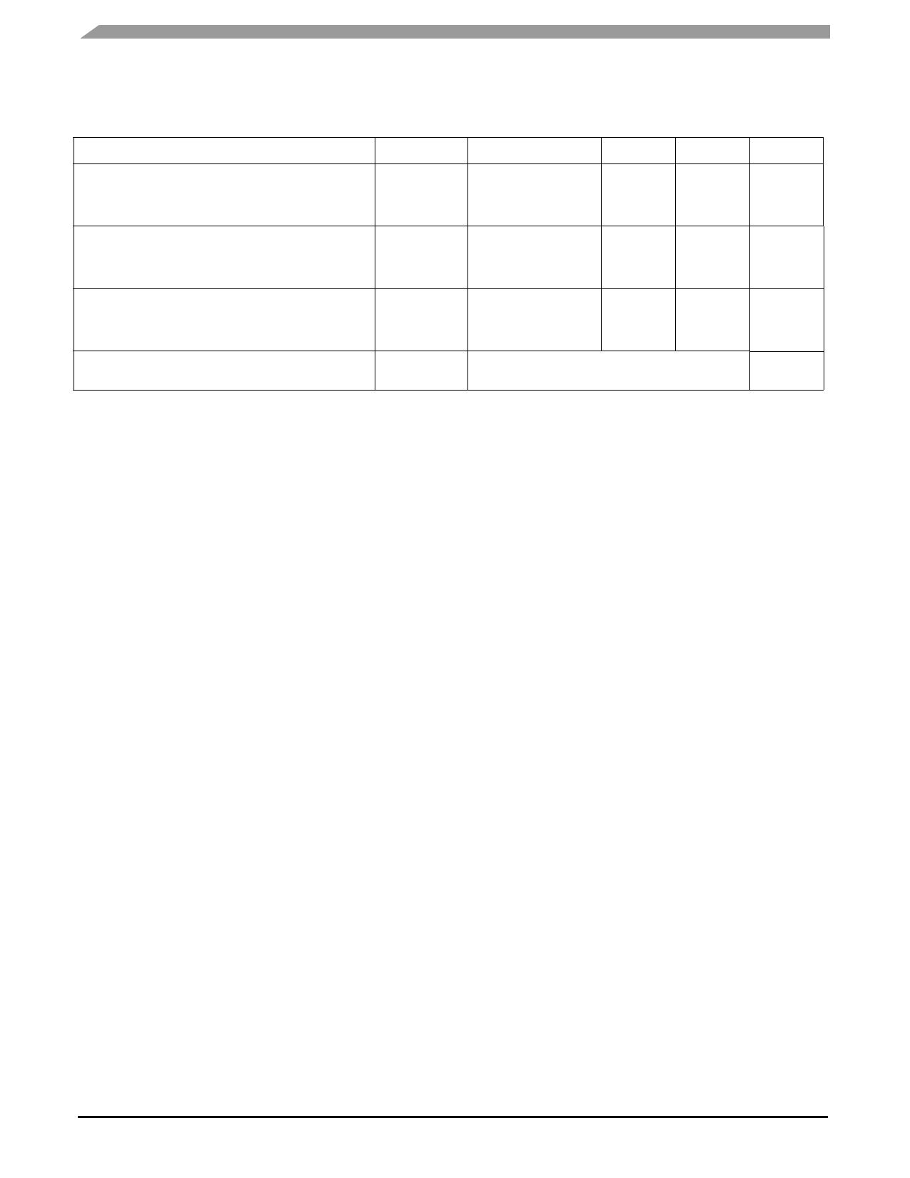
DEVICE VARIATIONS
DEVICE VARIATIONS
Table 1. Device Variations
Characteristic
Wake Input Clamp Voltage, ICL(WAKE) < 2.5 mA
10XS3412CHFK
10XS3412DHFK
Fault Detection Blanking Time
10XS3412CHFK
10XS3412DHFK
Output Shutdown Delay Time
10XS3412CHFK
10XS3412DHFK
Peak Package Reflow Temperature During Reflow(1),
(2)
Symbol
VCL(WAKE)
tFAULT
tDETECT
TPPRT
Min
Typ
Max
Unit
V
19
25
32
20
27
35
μs
-
5.0
20
-
5.0
10
μs
-
7.0
30
-
7.0
20
Note 2
°C
Notes
1. Pin soldering temperature limit is for 40 seconds maximum duration. Not designed for immersion soldering. Exceeding these limits may
cause malfunction or permanent damage to the device.
2. Freescale’s Package Reflow capability meets Pb-free requirements for JEDEC standard J-STD-020C. For Peak Package Reflow
Temperature and Moisture Sensitivity Levels (MSL), Go to www.freescale.com, search by part number [e.g. remove prefixes/suffixes
and enter the core ID to view all orderable parts (i.e. MC33xxxD enter 33xxx), and review parametrics.
10XS3412
2
Analog Integrated Circuit Device Data
Freescale Semiconductor
Share Link: 