APX9267X 데이터 시트보기 (PDF) - Anpec Electronics
부품명
상세내역
일치하는 목록
APX9267X Datasheet PDF : 12 Pages
| |||
APX9267
Pin Description
PIN
No.
Name
1
OUT2
2
VCC
3
IN+
4
IN-
5
FG
6
PWM
7
OUT1
8
GND
Description
H-bridge Output Connection. The output stage is a H-bridge formed by four transistors and
four-protection diode for switching applications.
Supply Voltage Input Pin.
Hall Input +.
Hall Input -.
Rotation Speed Output.
PWM Signal Input Terminal.
H-bridge Output Connection. The output stage is a H-bridge formed by four transistors and
four-protection diode for switching applications.
Ground.
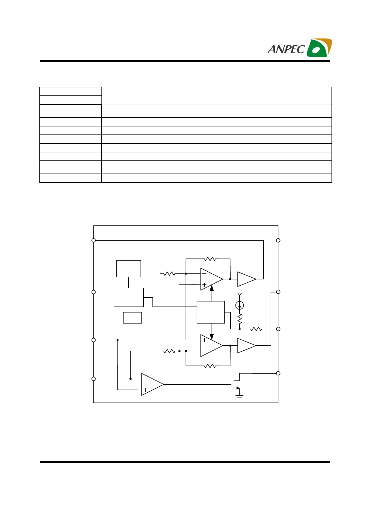
Block Diagram
OUT2
VCC
IN+
IN-
OSC
Lock
Protection
TSD
500Ω
500Ω
150kΩ
GND
Control
Vcc
5µA
90KΩ
10kΩ
OUT1
PWM
150kΩ
FG
Copyright © ANPEC Electronics Corp.
5
Rev. A.6 - Mar., 2008
www.anpec.com.tw
Share Link: 