CS8121 데이터 시트보기 (PDF) - Cherry semiconductor
부품명
상세내역
일치하는 목록
CS8121 Datasheet PDF : 8 Pages
| |||
Typical Performance Characteristics: continued
Quiescent Current vs. Output Current Over Temperature
Output Voltage and Supply Current vs. Input Voltage
3.5
3.0
-40°C
2.5
25°C
2.0
125°C
1.5
1.0
0.5
VIN = 14V
0.0
0
0.1
0.2
0.3
0.4
0.5
0.6
0.7
0.8
0.9
1.0
IOUT
5.5
5.0
4.0
3.0
2.0
1.0
0.0
0.0
VOUT
IQ
2.0
4.0
6.0
8.0
Supply Voltage
22.0
20.0
16.0
12.0
8.0
4.0
0.0
10.0
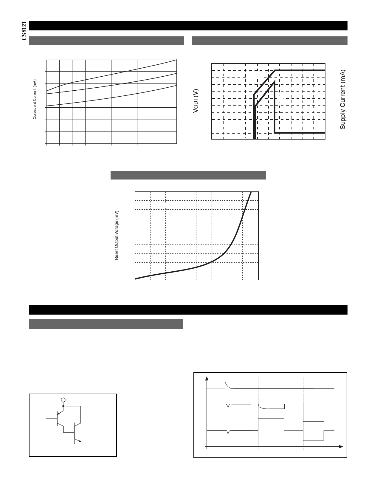
RESET Output Voltage vs. Output Current
2000
1800
1600
1400
1200
1000
800
600
400
200
0
1
VIN = 5V
5
10
15
20
25
30
35
40
Reset Output Current (mA)
Circuit Description
Voltage Reference and Output Circuitry
Precision Voltage Reference
The regulated output voltage depends on the precision
band gap voltage reference in the IC. By adding an error
amplifier into the feedback loop, the output voltage is
maintained within ±4% over temperature and supply vari-
ation.
The NPN pass device prevents deep saturation of the output
stage which in turn improves the ICÕs efficiency by prevent-
ing excess current from being used and dissipated by the IC.
Output Stage Protection
The output stage is protected against overvoltage, short
circuit and thermal runaway conditions (Figure 2).
> 30V
Output Stage
The composite PNP-
VIN
NPN output structure
(Figure 1) provides 1A
(typ) of output current
while maintaining a
low drop out voltage
(1.2V) and drawing lit-
tle quiescent current
(4mA).
VOUT
Figure 1. Composite Output Stage of the CS8121
VIN
VOUT
IOUT
Load
Dump
Short
Circuit
Thermal
Shutdown
Figure 2. Typical Circuit Waveforms for Output Stage Protection.
4
Share Link: 